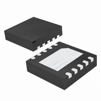
MAX8794ETB+T Maxim Integrated Products, MAX8794ETB+T Datasheet

MAX8794ETB+T
Specifications of MAX8794ETB+T
Related parts for MAX8794ETB+T
MAX8794ETB+T Summary of contents
Page 1
... PGOOD TDFN 3mm x 3mm *EXPOSED PAD. ________________________________________________________________ Maxim Integrated Products For pricing, delivery, and ordering information, please contact Maxim Direct at 1-888-629-4642, or visit Maxim’s website at www.maxim-ic.com. o Internal Power MOSFETs with Current Limit (3A typ) o Fast Load-Transient Response o External Reference Input with Reference = 1 ...
Page 2
Low-Voltage DDR Linear Regulator ABSOLUTE MAXIMUM RATINGS IN to PGND............................................................-0.3V to +4.3V OUT to PGND ..............................................-0. OUTS to AGND ............................................-0. AGND.........................................................-0.3V to +4.3V CC REFIN, REFOUT, SHDN, PGOOD to AGND...-0. PGND to ...
Page 3
Low-Voltage DDR Linear Regulator ELECTRICAL CHARACTERISTICS (continued 1.8V 3.3V REFIN OUTS Typical values are +25°C.) (Note 1) A PARAMETER SYMBOL REFERENCE REFIN Voltage Range V REFIN Input Bias ...
Page 4
Low-Voltage DDR Linear Regulator (Circuit of Figure +25°C, unless otherwise noted.) A OUTPUT LOAD REGULATION 0. 0.9V REFIN 0.94 0. 1.25V IN 0.90 0. 1.5V IN 0.86 0. ...
Page 5
Low-Voltage DDR Linear Regulator (Circuit of Figure +25°C, unless otherwise noted.) A REFOUT VOLTAGE ERROR vs. REFOUT LOAD CURRENT -10 -15 -20 - REFOUT LOAD CURRENT (mA) SHUTDOWN WAVEFORM ...
Page 6
Low-Voltage DDR Linear Regulator (Circuit of Figure +25°C, unless otherwise noted.) A DYNAMIC OUTPUT-VOLTAGE TRANSIENT 20.0µs/div SINK CURRENT-LIMIT DISTRIBUTION 50 SAMPLE SIZE = 200 -4.0 -3.5 -3.0 SINK CURRENT LIMIT (A) 6 ...
Page 7
Low-Voltage DDR Linear Regulator PIN NAME Buffered Reference Output. The output of the unity-gain reference input buffer sources and sinks over 1 REFOUT 5mA. Bypass REFOUT to AGND with a 0.33µF or greater ceramic capacitor. Analog Supply Input. Connect to ...
Page 8
Low-Voltage DDR Linear Regulator Detailed Description The MAX8794 is a low-voltage, low-dropout DDR termi- nation linear regulator with an external bias supply input and a buffered reference output (see Figures 1 and 2 powered by a 2.7V to ...
Page 9
Low-Voltage DDR Linear Regulator The MAX8794 features an open-drain PGOOD output that transitions high 2ms after the output initially reach- es regulation. PGOOD goes low within 10µs of when the output goes out of regulation by ±150mV. The MAX8794 features ...
Page 10
Low-Voltage DDR Linear Regulator 200μs SHDN CURRENT LIMIT POWER-GOOD WINDOW OUT 2ms STARTUP DELAY PGOOD Figure 3. MAX8794 PGOOD and Soft-Start Waveforms Power-Good (PGOOD) The MAX8794 provides an open-drain PGOOD output that goes high 2ms (typ) after the output initially ...
Page 11
Low-Voltage DDR Linear Regulator For a step-voltage change at REFIN, the rate of change of the output voltage is limited by the total output capacitance, the current limit, and the load during the transition. Adding a capacitor across REFIN and ...
Page 12
Low-Voltage DDR Linear Regulator Noise, PSRR, and Transient Response The MAX8794 operates with low-dropout voltage and low quiescent current in notebook computers while maintaining good noise, transient response, and AC- rejection specifications. Improved supply-noise rejec- tion and transient response can ...
Page 13
... Maxim cannot assume responsibility for use of any circuitry other than circuitry entirely embodied in a Maxim product. No circuit patent licenses are implied. Maxim reserves the right to change the circuitry and specifications without notice at any time. Maxim Integrated Products, 120 San Gabriel Drive, Sunnyvale, CA 94086 408-737-7600 ____________________ 13 © 2010 Maxim Integrated Products ...


