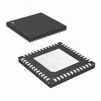
ISL6333IRZ Intersil, ISL6333IRZ Datasheet - Page 35

ISL6333IRZ
Manufacturer Part Number
ISL6333IRZ
Description
IC CTRLR PWM 3PHASE BUCK 48-QFN
Manufacturer
Intersil
Datasheet
1.ISL6333ACRZ.pdf
(40 pages)
Specifications of ISL6333IRZ
Applications
Controller, Intel VR11
Voltage - Input
5 ~ 12 V
Number Of Outputs
1
Voltage - Output
0.5 ~ 1.6 V
Operating Temperature
-40°C ~ 85°C
Mounting Type
Surface Mount
Package / Case
48-VQFN
Number Of Pwm Outputs
3
On/off Pin
Yes
Adjustable Output
Yes
Topology
Buck
Switching Freq
80 TO 1000kHz
Operating Supply Voltage (max)
5.25V
Output Current
100000A
Output Voltage
0.5 to 1.6V
Synchronous Pin
No
Rise Time
26ns
Fall Time
18ns
Operating Temperature Classification
Industrial
Mounting
Surface Mount
Pin Count
48
Package Type
QFN EP
Lead Free Status / RoHS Status
Lead free / RoHS Compliant
In Equation 40, L is the per-channel filter inductance divided
by the number of active channels; C is the sum total of all
output capacitors; ESR is the equivalent series resistance of
the bulk output filter capacitance; and V
peak-to-peak sawtooth signal amplitude, as described in the
“Electrical Specifications” on page 13.
Once selected, the compensation values in Equation 40
assure a stable converter with reasonable transient
performance. In most cases, transient performance can be
improved by making adjustments to R
value of R
oscilloscope until no further improvement is noted. Normally,
C
Equation 40 unless some performance issue is noted.
The optional capacitor C
noise away from the PWM comparator (see Figure 24). Keep
a position available for C
high-frequency capacitor of between 22pF and 150pF in
case any leading edge jitter problem is noted.
Case 3:
COMPENSATION WITHOUT LOAD-LINE REGULATION
The non load-line regulated converter is accurately modeled
as a voltage-mode regulator with two poles at the L-C
resonant frequency and a zero at the ESR frequency. A
type III controller, as shown in Figure 25, provides the
necessary compensation.
Case 2:
Case 1:
C
will not need adjustment. Keep the value of C
C
while observing the transient performance on an
------------------------------- -
2 π
R
C
C
C
⋅
R
C
------------------------------- -
2 π
f
R
C
C
C
⋅
=
=
0
⋅
1
C
C
>
=
=
R
-------------------------------------------------------------------------------------- -
(
⋅
L C
1
2 π
------------------------------------ -
2 π C ESR
=
=
FB
R
----------------------------------------------------- -
2 π V
⋅
⋅
L C
⋅
FB
R
----------------------------------------------------------------- -
2 π V
⋅
⋅
⋅
)
FB
⋅
≤
V
---------------------------------------------------------------- -
2
⋅
2
⋅
2
⋅
PP
f
⋅
, is sometimes needed to bypass
1
>
, and be prepared to install a
2 π f
----------------------------------------------------------
0
V
⋅
f
⋅
⋅
P-P
f
⋅
<
0
IN
2 π f
--------------------------------------------- -
V
0
2
⋅
P-P
35
------------------------------------ -
2 π C ESR
IN
(
⋅
⋅
2 π
⋅
⋅
⋅
⋅
V
V
ESR
V
R
⋅
0
⋅
P-P
⋅
IN
IN
R
FB
⋅
V
⋅
)
0
V
V
2
FB
IN
⋅
1
⋅
IN
P-P
⋅
ESR
⋅
⋅
⋅
ISL6333, ISL6333A, ISL6333B, ISL6333C
⋅
V
R
f
⋅
C
0
f
P-P
0
FB
C
f
2
. Slowly increase the
⋅
0
P-P
⋅
⋅
⋅
⋅
L C
L C
L
L
⋅
⋅
is the
L C
⋅
C
from
(EQ. 40)
The first step is to choose the desired bandwidth, f
compensated system. Choose a frequency high enough to
assure adequate transient performance but not higher than
1/3 of the switching frequency. The type-III compensator has
an extra high-frequency pole, f
added noise rejection or to assure adequate attenuation at
the error-amplifier high-order pole and zero frequencies. A
good general rule is to choose f
higher if desired. Choosing f
cause problems with too much phase shift below the system
bandwidth.
In the solutions to the compensation equations, there is a
single degree of freedom. For the solutions presented in
Equation 41, R
compensation components are then selected.
In Equation 41, L is the per-channel filter inductance divided
by the number of active channels; C is the sum total of all
output capacitors; ESR is the equivalent-series resistance of
the bulk output-filter capacitance; and V
peak-to-peak sawtooth signal amplitude, as described in the
“Electrical Specifications” on page 13.
Output Filter Design
The output inductors and the output capacitor bank together
to form a low-pass filter responsible for smoothing the
R
C
C
R
C
FIGURE 25. COMPENSATION CIRCUIT WITHOUT LOAD-LINE
1
1
2
C
C
=
=
=
=
=
C
R
R
------------------------------------------- -
---------------------------------------------------------------------------------------------------- -
(
---------------------------------------------------------------------------------------- -
---------------------------------------------------------------------------------------------------- -
(
V
2 π
1
2 π ⋅
1
L C
FB
PP
⋅
⋅
V
⋅
)
IN
⋅
)
V
R
2
------------------------------------------- -
2
–
⎛
⎝
IN
FB
⋅
2π
L C
⋅
⋅
REGULATION
C ESR
f
(
f
0
⋅
0
2 π f
FB
⎞
⎠
⋅
C ESR
⋅
⋅
(
2
⋅
⋅
2 π f
f
⋅
f
–
HF
⋅
HF
is selected arbitrarily. The remaining
⋅
R
f
C ESR
⋅
0
FB
R
⋅
⋅
HF
⋅
⋅
⋅
C
V
(
f
(
HF
HF
IN
C
⋅
L C
L C
2
⋅
⋅
⋅
⋅
C
L C
L C R
C
⋅
HF
) R
⋅
L C
) R
⋅
⋅
⋅
–
HF
⋅
to be lower than 10f
HF
1
FB
FB
–
)
. This pole can be used for
1
FB
COMP
VSEN
= 10f
⋅
)
⋅
V
V
FB
P-P
P-P
P-P
0
, but it can be
is the
ISL6333
October 8, 2010
0
0
, of the
(EQ. 41)
can
FN6520.3


