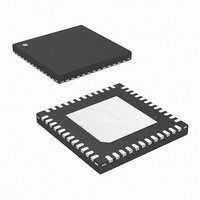
ISL6333AIRZ Intersil, ISL6333AIRZ Datasheet - Page 20

ISL6333AIRZ
Manufacturer Part Number
ISL6333AIRZ
Description
IC CTRLR PWM 3PHASE BUCK 48-QFN
Manufacturer
Intersil
Datasheet
1.ISL6333ACRZ.pdf
(40 pages)
Specifications of ISL6333AIRZ
Applications
Controller, Intel VR11
Voltage - Input
5 ~ 12 V
Number Of Outputs
1
Voltage - Output
0.5 ~ 1.6 V
Operating Temperature
-40°C ~ 85°C
Mounting Type
Surface Mount
Package / Case
48-VQFN
Rohs Compliant
YES
Lead Free Status / RoHS Status
Lead free / RoHS Compliant
Available stocks
Company
Part Number
Manufacturer
Quantity
Price
Company:
Part Number:
ISL6333AIRZ
Manufacturer:
Intersil
Quantity:
215
losses. The FS pin determines whether the controllers
operate in the coupled inductor mode or the standard
inductor mode of operation. Tying the FS pin resistor, R
to ground will set the controllers to operate in standard
inductor mode. Tying the R
controllers to operate in coupled inductor mode.
When PSI# is set LOW, the ISL6333 and ISL6333B also
utilize the new Gate Voltage Optimization Technology
(GVOT) to reduce Channel 1 lower MOSFET gate drive
voltage. The controllers are designed to optimize the
Channel 1 lower MOSFET gate drive voltage to ensure high
efficiency in both normal and low power states. In the low
power state where the converter load current is low,
MOSFET driving loss is a higher percentage of the power
loss associated with the lower MOSFET. In low power state,
the lower gate drive voltage can therefore be reduced to
decrease the driving losses of the lower MOSFETs and
increase the system efficiency. More information about this
can be found in the “Gate Voltage Optimization Technology
(GVOT) (ISL6333, ISL6333B Only)” on page 27.
When the PSI# pin is set HIGH, the controllers will
immediately begin returning the regulator to it’s normal
power state, by turning on all the active channels, placing
them in CCM mode, and increasing the Channel 1 lower
gate drive voltage back to it’s original level.
ISL6333A, ISL6333C LOW POWER STATE
On the ISL6333A and ISL6333C, when the PSI# pin is set
LOW, the controllers change their operating state by turning
off all active channels accept for Channel 1. This is the only
change made to the regulator. Channel 1 continues to
operate in CCM just as it does in the normal power state.
When the PSI# pin is set HIGH, the controllers immediately
begin returning the regulator to it’s normal power state, by
turning on all the active channels.
CPURST_N Operation (ISL6333B, ISL6333C Only)
The ISL6333B and ISL6333C both include a CPURST_N pin
which can be utilized by microprocessors that have a
CPURST_N output. The CPURST_N pin is a digital input
used in conjunction with the PSI# pin to indicate whether the
controllers should be in a lower power state of operation or
not. If CPURST_N is HIGH, the operating state of the
controllers is controlled by the PSI# pin. If CPURST_N is
LOW, the controllers will only run in their normal power state
and cannot be put into their light load power state. Once
CPURST_N toggles HIGH again, there is a 50ms delay
before the controllers recognize the state of the PSI# pin.
Channel Current Balance
One important benefit of multi-phase operation is the thermal
advantage gained by distributing the dissipated heat over
multiple devices and greater area. By doing this the designer
avoids the complexity of driving parallel MOSFETs and the
expense of using expensive heat sinks and exotic magnetic
materials.
FS
20
resistor to VCC sets the
ISL6333, ISL6333A, ISL6333B, ISL6333C
FS
,
In order to realize the thermal advantage, it is important that
each channel in a multi-phase converter be controlled to
carry equal amounts of current at any load level. To achieve
this, the currents through each channel must be sensed
continuously every switching cycle. The sensed currents,
I
divided by the number of active channels. The resulting
cycle average current, I
load-current demand on the converter during each switching
cycle. Channel current balance is achieved by comparing
the sensed current of each channel to the cycle average
current, and making the proper adjustment to each channel
pulse width based on the error. Intersil’s patented
current-balance method is illustrated in Figure 4, with error
correction for Channel 1 represented. In the figure, the cycle
average current, I
sensed current, I
The filtered error signal modifies the pulse width
commanded by V
I
correction is applied to each active channel.
SEN
ER
NOTE: CHANNEL 3 IS OPTIONAL.
V
COMP
FIGURE 4. CHANNEL-1 PWM FUNCTION AND
toward zero. The same method for error signal
, from each active channel are summed together and
FILTER
FIGURE 5. CONTINUOUS CURRENT SAMPLING
+
I
ER
CURRENT-BALANCE ADJUSTMENT
-
+
f(s)
I
SEN1
SEN1
COMP
AVG
-
I
AVG
PWM
, is compared with the Channel 1
, to create an error signal I
MODULATOR
AVG
WAVEFORM
to correct any unbalance and force
SWITCHING PERIOD
÷ N
RAMP
, provides a measure of the total
TIME
I
I
SEN
L
Σ
+
-
PWM1
I
I
SEN3
SEN2
ER
October 8, 2010
TO GATE
CONTROL
LOGIC
.
FN6520.3


