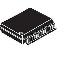
MCZ34702EWR2 Freescale Semiconductor, MCZ34702EWR2 Datasheet - Page 4

MCZ34702EWR2
Manufacturer Part Number
MCZ34702EWR2
Description
IC PWR SUPPLY 3A SW 32-SOIC
Manufacturer
Freescale Semiconductor
Datasheet
1.MC34702EK.pdf
(39 pages)
Specifications of MCZ34702EWR2
Applications
Controller, Power QUICC™ I, II
Voltage - Input
2.8 ~ 6 V
Number Of Outputs
2
Voltage - Output
7.75V, 0.8 ~ 6 V
Operating Temperature
-40°C ~ 85°C
Mounting Type
Surface Mount
Package / Case
32-SOIC (7.5mm Width)
Output Current
3 A
Input Voltage
2.8 V to 6 V
Switching Frequency
300 KHz
Mounting Style
SMD/SMT
Duty Cycle (max)
95 %
Lead Free Status / RoHS Status
Lead free / RoHS Compliant
Table 1.
4
34702
PIN CONNECTIONS
A functional description of each pin can be found in the
Pin
20
21
22
23
26
27
28
29
30
31
32
Pin Function Description (continued)
Pin Name
CLKSYN
CLKSEL
ADDR
LDRV
VDDI
VIN1
RST
EN1
EN2
CS
RT
Clock Synchronization
Clock Selection
Input Voltage 1
Formal Name
Current Sense
Power Supply
Reset Output
(Active LOW)
Linear Drive
Reset Timer
Enable 1
Enable 2
Address
Current sense pin of the LDO. Over-current protection of the linear regulator external
power MOSFET. The voltage drop over the LDO current sense resistor RS is sensed
between the CS and LDO pins. The LDO current limit can be adjusted by selecting
the proper value of the current sensing resistor RS.
LDO gate drive of the external pass N-channel MOSFET.
The input supply pin for the integrated circuit. The internal circuits of the IC are
supplied through this pin.
Internal supply voltage. A ceramic low ESR 1uF 6V X5R or X7R capacitor is
recommended.
I
through a 10kΩ resistor.
Enable 1 Input. The combination of the logic state of the Enable 1 and Enable 2
inputs determines operation mode and type of power sequencing of the IC.
Enable 2 Input. The combination of the logic state of the Enable 1 and Enable 2
inputs determines operation mode and type of power sequencing of the IC.
This pin allows programming of the Power-ON Reset delay by means of an external
RC network.
The reset control circuit monitors both the switching regulator and the LDO feedback
voltages. It is an open drain output and has to be pulled up to some supply voltage
(e.g., the output of the LDO) by an external resistor.
This pin sets the CLKSYN pin as either an oscillator output or a synchronization input
pin. The CLKSEL pin is also used for the I
Oscillator output/synchronization input pin.
2
C address selection. This pin can either be left open, tied to V
Functional Pin Description
Definition
section beginning on
Analog Integrated Circuit Device Data
2
C address selection.
Freescale Semiconductor
page
DDI
, or grounded
16.


