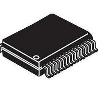
MCZ34702EWR2 Freescale Semiconductor, MCZ34702EWR2 Datasheet - Page 27

MCZ34702EWR2
Manufacturer Part Number
MCZ34702EWR2
Description
IC PWR SUPPLY 3A SW 32-SOIC
Manufacturer
Freescale Semiconductor
Datasheet
1.MC34702EK.pdf
(39 pages)
Specifications of MCZ34702EWR2
Applications
Controller, Power QUICC™ I, II
Voltage - Input
2.8 ~ 6 V
Number Of Outputs
2
Voltage - Output
7.75V, 0.8 ~ 6 V
Operating Temperature
-40°C ~ 85°C
Mounting Type
Surface Mount
Package / Case
32-SOIC (7.5mm Width)
Output Current
3 A
Input Voltage
2.8 V to 6 V
Switching Frequency
300 KHz
Mounting Style
SMD/SMT
Duty Cycle (max)
95 %
Lead Free Status / RoHS Status
Lead free / RoHS Compliant
Table 8.
DATA Definition
several Command Bytes. The Command Byte identifies the
kind of operation required by the master to be performed and
has two fields, as illustrated in
The address field is selected from the list in
field definitions for the entire set of operation options.
Table 7.
Analog Integrated Circuit Device Data
Freescale Semiconductor
Voltage Margining
LDO Output: x = 0
Command Byte)
Switcher Output
1. Address field
2. Value field
The DATA field in the single Data Transfer contains one or
Refer to
Address Field
Operation
(As a 2nd
x
001
011
= 1
Command Byte Definitions
Address Field Definitions
Table
Figure 23. Command Byte
Address Field
8, page 27, which summarizes the value
MSB
D7
0
0
0
0
0
0
0
0
0
0
0
0
0
0
0
0
7
Address
Voltage Margining
D6 D5 D4 D3
0
0
0
0
0
0
0
0
0
0
0
0
0
0
0
0
6
Operation
Watchdog
1
1
1
1
1
1
1
1
1
1
1
1
1
1
1
1
5
0
x
x
x
x
x
x
x
x
x
x
x
x
x
x
x
Figure
4
Bits
0
0
0
0
0
0
0
0
0
1
1
1
1
1
1
1
Value Field
3
Value
0
0
0
0
0
1
1
1
1
0
0
0
0
1
1
1
23:
D2
2
0
0
0
1
1
0
0
1
1
0
0
1
1
0
0
1
D1 D0
1
Table
0 1st Command
0
1
0
1
0
1
0
1
0
1
0
1
0
1
0
LSB
0
Write
W
W
Nominal
7.
Action
+ 1.0%
+ 2.0%
+ 3.0%
+ 4.0%
+ 5.0%
+ 6.0%
+ 7.0%
Output
- 1.0%
- 2.0%
- 3.0%
- 4.0%
- 5.0%
- 6.0%
- 7.0%
Table 8.
Table 9.
Security in Writing Commands
defined to initiate each write communications. The first
command identifies the operation, which is executed by the
following command byte.
operation one, followed by a null value field (all zeros).
Table 9
sends the first command before the command byte for the
intended operation.
VOLTAGE MARGINING OPERATION
master sends the first command followed by the specific
command byte to set the required voltage margining for either
the LDO or the switcher (see
simultaneous set for both LDO and switcher, two specific
commands must be issued in sequence after the first
command, one for each supply.
Notes
Command Byte)
24.
Programming
To improve the security level, a so-called first command is
A first command has the address field equal to the related
After starting the communication in Writing Mode, the
Watchdog
(As a 2nd
First Command
The watchdog timer is turned ON automatically after
receiving any other valid command byte changing the
watchdog time.
001 00000
011 00000
summarizes first command definitions. The master
Command Byte Definitions
First Command Definitions
0
0
0
0
0
0
0
0
0
0
1
1
1
1
1
1
1
1
1
1
LOGIC COMMANDS AND REGISTERS
1
1
1
1
1
1
1
1
1
1
FUNCTIONAL DEVICE OPERATION
Figure
0
0
0
0
0
0
0
0
0
0
Watchdog Programming
0
0
1
1
1
1
1
1
1
1
Voltage Margining
24). To achieve a
0
0
0
0
0
0
1
1
1
1
Operation
0
0
0
0
1
1
0
0
1
1
0 1st Command
0
0
1
0
1
0
1
0
1
WD 1280ms
WD 1280ms
WD 320ms
WD 320ms
Wind. OFF
Wind. OFF
Wind. OFF
Wind. OFF
WD 80ms
WD 20ms
Wind. ON
Wind. ON
WD 80ms
Wind. ON
WD 20ms
Wind. ON
WD OFF
(24)
34702
27


