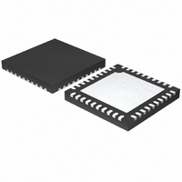
ISL6260CCRZ Intersil, ISL6260CCRZ Datasheet - Page 21

ISL6260CCRZ
Manufacturer Part Number
ISL6260CCRZ
Description
IC REG PWM MULTI-PHASE 40-QFN
Manufacturer
Intersil
Datasheet
1.ISL6260CCRZ.pdf
(28 pages)
Specifications of ISL6260CCRZ
Applications
Converter, Intel IMVP-6
Number Of Outputs
1
Voltage - Output
0.3 ~ 1.5 V
Operating Temperature
-10°C ~ 100°C
Mounting Type
Surface Mount
Package / Case
40-VFQFN, 40-VFQFPN
Lead Free Status / RoHS Status
Lead free / RoHS Compliant
Voltage - Input
-
Available stocks
Company
Part Number
Manufacturer
Quantity
Price
Company:
Part Number:
ISL6260CCRZ
Manufacturer:
Intersil
Quantity:
100
Part Number:
ISL6260CCRZ
Manufacturer:
INTERSIL
Quantity:
20 000
determine the choice of the SOFT capacitor, C
Equation 1:
Using a SLEWRATE of 10mV/µs, and the typical I
given in the Table Electrical Specifications on page 4 of
205µA, C
A choice of 0.015µF would guarantee a SLEWRATE of
10mV/µs is met for minimum I
“Electrical Specifications” table on page 4.
Now this choice of C
slewrate as well. One should expect the output voltage to
slew to the Boot value of 1.2V at a rate given by Equation 3:
Generally, when output voltage is approaching its steady
state, its dv/dt will slow down to prevent overshoot. In order
to compensate the slow-down effect, faster initial dv/dt slew
rates can be used with small soft capacitors such as 10nF to
achieve the desired overall dv/dt in the allocated time
interval.
Selecting R
To properly bias the ISL6260C, a reference current is
established by placing a 147kΩ, 1% tolerance resistor from
the R
10μA current source from which OCSET reference current
can be derived.
Care should be taken in layout that the resistor is placed
very close to the R
ground is connected to the opposite side of the R
resistor. Do not connect any other components to this pin.
Capacitance on this pin would create instabilities and should
be avoided.
Start-up Operation - CLK_EN# and PGOOD
The ISL6260C provides a 3.3V logic output pin for
CLK_EN#. The 3V3 pin allows for a system 3.3V source to
be connected to separated circuitry inside the ISL6260C,
solely devoted to the CLK_EN# function. The output is a
3.3V CMOS signal with 4mA of source and sinking
capability. This implementation removes the need for an
external pull-up resistor on this pin, and due to the normal
level of this signal being a low, removes the leakage path
from the 3.3V supply to ground through the pull-up resistor.
This reduces 3.3V supply current, that would occur under
normal operation with a pull-up resistor, and prolongs battery
life. The 3.3V supply should be decoupled to digital ground,
not to analog ground for noise immunity.
C
dV
-------
dt
C
SOFT
SOFT
=
BIAS
------------------ -
C
SOFT
=
I
SS
SOFT
=
----------------------------------- -
SLEWRATE
pin to ground. This will provide a highly accurate,
205μA
----------------- -
10mV
--------------- -
1μs
BIAS
=
I
is:
GV
---------------------- -
0.015μF
42μA
=
BIAS
SOFT
0.0205μF
pin and that a good quality signal
=
will then control the start-up
2.8
21
GV
mV
-------- -
μs
value, given in the
SOFT
GV
BIAS
, by
value,
(EQ. 1)
(EQ. 2)
(EQ. 3)
ISL6260C
As mentioned in the “Theory of Operation” on page 17 of this
datasheet, CLK_EN# is logic level high at start-up. When the
output voltage reaches 90% of Boot voltage, a counter is
enabled, it counts 13 switching cycles, about 43µs for
300kHz operation, then CLK_EN# goes low. This in turn
triggers an internal timer for the IMVP-6+_PWRGD signal.
This timer allows IMVP-6+_PWRGD to go high
approximately 7ms after CLK_EN# goes low.
Static Mode of Operation - Processor Die Sensing
Die sensing allows the Voltage Regulator to compensate for
various resistive drops in the power path and insure that the
voltage seen at the CPU die is the correct level independent
of load current.
The VSEN and RTN pins of the ISL626C are connected to
Kelvin sense leads at the die of the processor through the
processor socket. These signal names are V
V
to tightly control the processor voltage at the die,
independent of layout inconsistencies and drops. This Kelvin
sense technique provides for extremely tight load line
regulation.
These traces should be laid out as noise sensitive traces.
For optimum load line regulation performance, the traces
connecting these two pins to the Kelvin sense leads of the
processor must be laid out in parallel and away from rapidly
rising voltage nodes (switching nodes) and other noisy
traces. To achieve optimum performance, place common
mode and differential mode RC filters to analog ground on
VSEN and RTN as shown in Figure 46. However, the filter
resistors should be in order of 10Ω so that they do not
interact with the 50kΩ input resistance of the differential
amplifier.
Due to the fact that the voltage feedback to the switching
regulator is sensed at the processor die, there exists the
potential of an overvoltage due to an open circuit feedback
signal, should the regulator be operated without the
processor installed. Due to this fact, we recommend the use
of the Ropn1 and Ropn2 connected to V
shown in Figure 46. These resistors will provide voltage
feedback in the event that the system is powered up without
a processor installed. These resistors are typically 100Ω.
Setting the Switching Frequency - FSET
The R
architecture. The switching frequency can increase during
the application of a load to improve transient performance.
However, it also varies slightly due changes in input and
output voltage and output current, but this variation is
normally less than 10% in continuous conduction mode.
Refer to Figure 39. A resistor connected between the VW
and COMP pins of the ISL6260C adjusts the switching
window, and therefore adjusts the switching frequency. The
Rfset resistor that sets up the switching frequency of the
CC_SENSE
3
modulator scheme is not a fixed frequency PWM
respectively. This allows the Voltage Regulator
OUT
CC_SENSE
and ground as
June 21, 2010
FN9259.3
and


