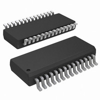
ISL6539IAZ-T Intersil, ISL6539IAZ-T Datasheet - Page 17

ISL6539IAZ-T
Manufacturer Part Number
ISL6539IAZ-T
Description
IC CTRLR DDR DRAM, SDRAM 28QSOP
Manufacturer
Intersil
Datasheet
1.ISL6539CAZ.pdf
(20 pages)
Specifications of ISL6539IAZ-T
Applications
Controller, DDR DRAM, SDRAM
Voltage - Input
3.3 ~ 18 V
Number Of Outputs
2
Voltage - Output
0.9 ~ 5.5 V
Operating Temperature
-40°C ~ 85°C
Mounting Type
Surface Mount
Package / Case
28-QSOP
Lead Free Status / RoHS Status
Lead free / RoHS Compliant
The total power loss of the upper MOSFET is the sum of the
switching loss and the conduction loss. The temperature rise
on the MOSFET can be calculated based on the thermal
impedance given on the datasheet of the MOSFET. If the
temperature rise is too much, a different MOSFET package
size, layout copper size, and other options have to be
considered to keep the MOSFET cool. The temperature rise
can be calculated by Equation 28:
The MOSFET gate driver loss can be calculated with the
total gate charge and the driver voltage Vcc. The lower
MOSFET only charges the miller capacitor at turn-off.
Based on Equation 29, the system efficiency can be
estimated by the designer.
Confining the Negative Phase Node Voltage Swing
with Schottky Diode
At each switching cycle, the body diode of the lower MOSFET
will conduct before the MOSFET is turned-on, as the inductor
current is flowing to the output capacitor. This will result in a
negative voltage on the phase node. The higher the load
current, the lower this negative voltage. This voltage will ring
back less negative when the lower MOSFET is turned on.
A total 400ns period is given to the current sample-and-hold
circuit on the ISEN pin to sense the current going through
the lower MOSFET after the upper MOSFET turns off. An
excessive negative voltage on the lower MOSFET will be
treated as overcurrent. In order to confine this voltage, a
Schottky diode can be used in parallel with the lower
MOSFET for high load current applications. PCB layout
parasitics should be reduced in order to reduce the negative
ringing of phase voltage.
Another concern for the phase node voltage going into
negative is that the boot strap capacitor between the BOOT
and PHASE pin could get be charged higher than VCC
voltage, exceeding the 6.5V absolute maximum voltage
between BOOT and PHASE when the phase became
negative. A resistor can be placed between the cathode of
the boot strap diode and BOOT pin to increase the charging
time constant of the boot cap. This resistor will not affect the
turn-on and off of the upper MOSFET.
A Schottky diode can reduce the reverse recovery of the lower
MOSFET when transitioning from freewheeling to blocking,
therefore, it is generally good practice to have a Schottky
diode closely parallel with the lower MOSFET. B340LA, from
Diodes, Inc.®, can be used as the external Schottky diode.
Tuning the Turn-on of Upper MOSFET
The turn-on speed of the upper MOSFET can be adjusted by
the resistor connecting the boot cap to the boot pin of the chip.
This resistor can confine the voltage ringing on the boot
T
P
rise
driver
=
=
θ P
ja totalpower loss
V
cc
Q
gs
f
sw
17
(EQ. 28)
(EQ. 29)
ISL6539
capacitor from coupling to the boot pin. This resistor slows
down only the turn-on of the upper MOSFET. If the upper
MOSFET is turned on very fast, it could result in a very high
dv/dt on the phase node, which could couple into the lower
MOSFET gate through the miller capacitor, causing
momentous shoot-through. This phenomenon, together with
the reverse recovery of the body diode of the lower MOSFET,
can overshoot the phase node voltage to beyond the voltage
rating of the MOSFET. However, a bigger resistor will slow the
turn-on of the MOSFET too much and lower the efficiency.
Trade-offs need to be made in choosing such a resistor.
System Loop Gain and Stability
The system loop gain is a product of three transfer functions:
These transfer functions are written in a closed form in
“Theory of Operation” on page 9. The external capacitor, in
parallel with the upper resistor of the resistor divider, C
be used to tune the loop gain and phase margin. Other
component parameters, such as the inductor value, can be
changed for a wider cross-over frequency of the system loop
gain. A body plot of the loop gain transfer function with a 45°
phase margin (a 60° phase margin is better) is desirable to
cover component parameter variations.
Testing the Overvoltage on Buck Converters
For synchronous buck converters, if an active source is used
to raise the output voltage for the overvoltage protection test,
the buck converter will behave like a boost converter and
dump energy from the external source to the input. The
overvoltage test can be done on ISL6539 by connecting the
VSEN pin to an external voltage source or signal generator
through a diode. When the external voltage (or signal
generator voltage) is tuned to a higher level than the
overvoltage threshold (the lower MOSFET will be on), it
indicates the overvoltage protection works. This kind of
overvoltage protection does not require an external Schottky
in parallel with the output capacitor.
Layout Considerations
Power and Signal Layer Placement on the PCB
As a general rule, power layers should be close together,
either on the top or bottom of the board, with signal layers on
the opposite side of the board. For example, prospective
layer arrangement on a 4-layer board is shown in the
following:
1. the transfer function from the output voltage to the
2. the transfer function of the internal compensation circuit
3. and the transfer function from the error amplifier output to
1. Top Layer: ISL6539 signal lines
2. Signal Ground
feedback point,
from the feedback point to the error amplifier output
voltage,
the converter output voltage.
April 29, 2010
FN9144.6
z
, can


