ISL6336ACRZ Intersil, ISL6336ACRZ Datasheet
ISL6336ACRZ
Specifications of ISL6336ACRZ
Available stocks


Related parts for ISL6336ACRZ

ISL6336ACRZ Summary of contents
Page 1
... CAUTION: These devices are sensitive to electrostatic discharge; follow proper IC Handling Procedures. | 1-888-INTERSIL or 1-888-468-3774 Intersil (and design registered trademark of Intersil Americas Inc. Copyright Intersil Americas Inc. 2008, 2009. All Rights Reserved All other trademarks mentioned are the property of their respective owners. FN6504.1 ...
Page 2
... NUMBER ISL6336CRZ* ISL6336 CRZ ISL6336IRZ* ISL6336 IRZ ISL6336ACRZ* ISL6336A CRZ ISL6336AIRZ * ISL6336A IRZ *Add “-T” for tape and reel. Please refer to TB347 for details on reel specifications. NOTE: These Intersil Pb-free plastic packaged products employ special Pb-free material sets, molding compounds/die attach materials, and 100% matte tin plate plus anneal (e3 termination finish, which is RoHS compliant and compatible with both SnPb and Pb-free soldering operations) ...
Page 3
... Quad Output (Two Phase) ISL6610 5V Quad Output (Two Phase) NOTE: Intersil 5V and 12V drivers are mostly pin-to-pin compatible and allow dual footprint layout to optimize MOSFET selection and efficiency. Dual = One Synchronous Channel; Quad = Two Synchronous channels. 3 ISL6336, ISL6336A COMMENTS DIODE GATE DRIVE ...
Page 4
ISL6336, ISL6336A Block Diagram VDIFF VR_RDY RGND x1 VSEN OVP SOFT-START +175mV FAULT LOGIC SS OFS OFFSET REF DAC VID7 VID6 VID5 DYNAMIC VID4 VID DAC VID3 VID2 VID1 VID0 COMP FB 1.12V OC2 IMON 1.12V 4 ISL6336, ISL6336A OVP ...
Page 5
Typical Application - 5-Phase Buck Converter with DCR Sensing and Integrated TCOMP FB COMP APA REF DAC VDIFF VSEN VCC RGND GND VTT EN_VTT VR_RDY ISL6336 VID7 PWM1 VID6 ISEN1- VID5 ISEN1+ VID4 PWM4 VID3 ISEN4- VID2 ISEN4+ VID1 VID0 ...
Page 6
Typical Application - 4-Phase Buck Converter with coupled inductors COMP APA REF FB DAC VDIFF VSEN VCC RGND GND VTT EN_VTT VR_RDY ISL6336 VID7 PWM1 VID6 ISEN1- VID5 ISEN1+ VID4 PWM3 VID3 ISEN3- VID2 ISEN3+ VID1 VID0 PWM2 PSI# ISEN2- ...
Page 7
... Operating Conditions Supply Voltage, VCC . . . . . . . . . . . . . . . . . . . . . . . . . . . . . +5V ±5% Ambient Temperature ISL6336ACRZ, ISL6336CRZ . . . . . . . . . . . . . . . . . . 0°C to +70°C ISL6336AIRZ, ISL6336IRZ .-40°C to +85°C CAUTION: Do not operate at or near the maximum ratings listed for extended periods of time. Exposure to such conditions may adversely impact product reliability and result in failures not covered by warranty. ...
Page 8
Electrical Specifications Operating Conditions: VCC = 5V, Unless Otherwise Specified. Parameters with MIN and/or MAX limits are 100% tested at +25°C, unless otherwise specified. Temperature limits established by characterization and are not production tested. (Continued) PARAMETER PIN-ADJUSTABLE OFFSET Voltage at ...
Page 9
Electrical Specifications Operating Conditions: VCC = 5V, Unless Otherwise Specified. Parameters with MIN and/or MAX limits are 100% tested at +25°C, unless otherwise specified. Temperature limits established by characterization and are not production tested. (Continued) PARAMETER THERMAL MONITORING AND FAN ...
Page 10
... A capacitor is used between REF and ground to smooth the voltage transition during Dynamic VID™ operations. PWM[6:1] - Pulse width modulation outputs. Connect these pins to the PWM input pins of the Intersil driver IC. The number of active channels is determined by the state of PWM3, PWM4, PWM5, and PWM6. Tie PWM3 to VCC to configure for 2-phase operation ...
Page 11
OFS - The OFS pin provides a means to program a DC offset current for generating a DC offset voltage at the REF input. The offset current is generated via an external resistor and precision internal voltage references. The polarity ...
Page 12
... Figure 24 shows the single phase input-capacitor RMS current for comparison. PWM Modulation Scheme The ISL6336, ISL6336A adopts Intersil's proprietary Active Pulse Positioning (APP) modulation scheme to improve the transient performance. APP control is a unique dual-edge PWM modulation scheme with both PWM leading and trailing edges being independently moved to provide the best response to the transient loads ...
Page 13
... PWM potential, but not lower it below the Phase 1/2 level set by the controller IC. Therefore, the controller's - PWM outputs are directly compatible with Intersil drivers that require 5V PWM signal amplitudes. Drivers requiring 3.3V PWM signal amplitudes are generally incompatible. FS ...
Page 14
Current Sensing The ISL6336, ISL6336A senses current continuously for fast response. The ISL6336, ISL6336A supports inductor DCR sensing, or resistor sensing techniques. The associated channel current sense amplifier uses the ISEN inputs to reproduce a signal proportional to the inductor ...
Page 15
... Channel current balance is achieved by comparing the sensed current of each channel to the average current to make an appropriate adjustment to the PWM duty cycle of each channel with Intersil’s patented current-balance method. Channel current balance is essential in achieving the thermal advantage of multiphase operation. With good current balance, the power loss is equally dissipated over multiple devices and a greater area ...
Page 16
TABLE 3. VR11 VID 8-BIT (Continued) VID7 VID6 VID5 VID4 VID3 VID2 VID1 VID0 VOLTAGE ...
Page 17
TABLE 3. VR11 VID 8-BIT (Continued) VID7 VID6 VID5 VID4 VID3 VID2 VID1 VID0 VOLTAGE ...
Page 18
TABLE 3. VR11 VID 8-BIT (Continued) VID7 VID6 VID5 VID4 VID3 VID2 VID1 VID0 VOLTAGE ...
Page 19
... POR level before the ISL6336, ISL6336A becomes enabled. The schematic in Figure 8 demonstrates sequencing the ISL6336, ISL6336A with the ISL66xx family of Intersil MOSFET drivers, which require 12V bias. 3. The voltage on EN_VTT must be higher than 0.875V to enable the controller. This pin is typically connected to the output of the VTT voltage regulator ...
Page 20
VID voltage minus the offset voltage 500mV/DIV OUT EN_VTT VR_RDY 500µs/DIV FIGURE 9. SOFT-START WAVEFORMS The soft-start time is the sum of the 4 periods ...
Page 21
... At the inception of an overvoltage event, all PWM outputs are commanded low instantly (in less than 20ns). This causes the Intersil drivers to turn on the lower MOSFETs and pull the output voltage down to avoid damaging the load. When the voltage at VDIFF falls below the DAC plus 75mV, PWM signals enter a high-impedance state ...
Page 22
... IMON buffer. At the beginning of overcurrent shutdown, the controller places all PWM signals in a high-impedance state within 20ns commanding the Intersil MOSFET driver ICs to turn off both upper and lower MOSFETs. The system remains in this state for 4096 switching cycles (programmed switching frequency). If the controller is still enabled at the end of this wait period, it will attempt a soft-start ...
Page 23
VCC R 0.391V CC TM1 NTC 0.333V CC FIGURE 14. BLOCK DIAGRAM OF THERMAL MONITORING FUNCTION 100 TEMPERATURE (°C) FIGURE 15. THE RATIO ...
Page 24
Based on the VCC voltage, ISL6336, ISL6336A converts the TM pin voltage to a 6-bit digital signal for temperature compensation. With the non-linear A/D converter of ISL6336, ISL6336A, the TM digital signal is linearly proportional to the NTC temperature. For ...
Page 25
... It is assumed that the reader is familiar with many of the basic skills and techniques referenced in the following. In addition to this guide, Intersil provides complete reference designs that include schematics, bills of materials, and example board layouts for all common microprocessor applications ...
Page 26
Current Sensing Resistor The resistors connected to the ISEN+ pins determine the gains in the load-line regulation loop and the channel-current balance loop as well as setting the overcurrent trip point. Select values for these resistors by the Equation 32. ...
Page 27
C (OPTIONAL COMP DROOP - VDIFF FIGURE 19. COMPENSATION CONFIGURATION FOR LOAD-LINE REGULATED ISL6336, ISL6336A CIRCUIT The feedback resistor has already been chosen as FB outlined in “Load-Line ...
Page 28
C ESR ---------------------------------------- - ESR – ESR – ---------------------------------------- - 0.75V ------------------------------------------------------------------- - ...
Page 29
Filter Design” on page 28. Choose the lowest switching frequency that allows the regulator to meet the transient-response requirements. Switching frequency is determined by the selection of the frequency-setting resistor, R (see ...
Page 30
... Accordingly, the reader is cautioned to verify that data sheets are current before placing orders. Information furnished by Intersil is believed to be accurate and reliable. However, no responsibility is assumed by Intersil or its subsidiaries for its use; nor for any infringements of patents or other rights of third parties which may result from its use ...
Page 31
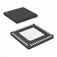
Package Outline Drawing L48.7x7 48 LEAD QUAD FLAT NO-LEAD PLASTIC PACKAGE Rev 4, 10/06 7.00 6 PIN 1 INDEX AREA (4X) 0.15 TOP VIEW ( TYP ) ( TYPICAL RECOMMENDED LAND PATTERN 31 ...