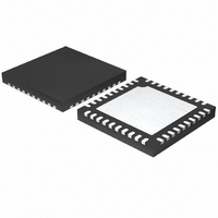
ISL6334DIRZ-T Intersil, ISL6334DIRZ-T Datasheet - Page 24

ISL6334DIRZ-T
Manufacturer Part Number
ISL6334DIRZ-T
Description
IC CTRLR PWM 4PHASE VR11.1 40QFN
Manufacturer
Intersil
Datasheet
1.ISL6334DCRZ-T.pdf
(28 pages)
Specifications of ISL6334DIRZ-T
Applications
Controller, Intel VR11.1
Voltage - Input
3 ~ 12 V
Number Of Outputs
1
Voltage - Output
0.5 ~ 1.6 V
Operating Temperature
-40°C ~ 85°C
Mounting Type
Surface Mount
Package / Case
40-VFQFN, 40-VFQFPN
Lead Free Status / RoHS Status
Lead free / RoHS Compliant
the power stage, since the DC resistance of the current
sense element may be changed according to the operational
temperature. R
resistance of the current sense element at the all operational
temperature.
In certain circumstances, it may be necessary to adjust the
value of one or more ISEN resistors. When the components
of one or more channels are inhibited from effectively
dissipating their heat so that the affected channels run hotter
than desired, choose new, smaller values of R
affected phases (see the section entitled “Voltage
Regulation” on page 13). Choose R
desired decrease in temperature rise in order to cause
proportionally less current to flow in the hotter phase, as
shown in Equation 28:
In Equation 28, make sure that ΔT
rise above the ambient temperature, and ΔT
temperature rise above the ambient temperature. While a
single adjustment according to Equation 28 is usually
sufficient, it may occasionally be necessary to adjust R
two or more times to achieve optimal thermal balance
between all channels.
Compensation
The ISL6334D converter can be accurately modeled as a
voltage-mode regulator with two poles at the L-C resonant
frequency and a zero at the ESR frequency. A type III
controller, as shown in Figure 17, provides the necessary
compensation.
The first step is to choose the desired bandwidth, f
compensated system. Choose a frequency high enough to
assure adequate transient performance but not higher than
1/3 of the switching frequency. The type III compensator has
an extra high-frequency pole, f
added noise rejection or to assure adequate attenuation at
the error-amplifier high-order pole and zero frequencies. A
good general rule is to choose f
R
ISEN 2 ,
C
R
1
1
=
R
FIGURE 17. COMPENSATION CIRCUIT
ISEN
X
in Equation 27 should be the maximum DC
ΔT
----------
ΔT
R
FB
R
2
1
C
C
2
C
C
24
HF
HF
2
. This pole can be used for
COMP
VSEN
ISEN,2
is the desired temperature
= 10f
FB
0
, but it can be
in proportion to the
1
is the measured
ISL6333
ISEN
0
for the
, of the
(EQ. 28)
ISEN
ISL6334D
higher if desired. Choosing f
cause problems with too much phase shift below the system
bandwidth.
In the solutions to the compensation equations, there is a
single degree of freedom. For the solutions presented in
Equation 29, R
The remaining compensation components are then selected.
In Equation 29, L is the per-channel filter inductance divided
by the number of active channels; C is the sum total of all
output capacitors; ESR is the equivalent-series resistance of
the bulk output-filter capacitance; and V
peak-to-peak sawtooth signal amplitude, typically 1.5V.
Output Filter Design
The output inductors and the output capacitor bank together
to form a low-pass filter responsible for smoothing the
pulsating voltage at the phase nodes. The output filter also
must provide the transient energy until the regulator can
respond. Because it has a low bandwidth compared to the
switching frequency, the output filter necessarily limits the
system transient response. The output capacitor must
supply or sink load current while the current in the output
inductors increases or decreases to meet the demand.
In high-speed converters, the output capacitor bank is usually
the most costly (and often the largest) part of the circuit.
Output filter design begins with minimizing the cost of this part
of the circuit. The critical load parameters in choosing the
output capacitors are the maximum size of the load step, ΔI;
the load-current slew rate, di/dt; and the maximum allowable
output-voltage deviation under transient loading, ΔV
Capacitors are characterized according to their capacitance,
ESR, and ESL (equivalent series inductance).
At the beginning of the load transient, the output capacitors
supply all of the transient current. The output voltage will initially
deviate by an amount approximated by the voltage drop across
the ESL. As the load current increases, the voltage drop across
the ESR increases linearly until the load current reaches its final
R
C
C
R
C
1
1
2
C
C
=
=
=
=
=
R
------------------------------------------- -
---------------------------------------------------------------------------------------------------- -
(
---------------------------------------------------------------------------------------- -
---------------------------------------------------------------------------------------------------- -
(
V
2 π
2 π ⋅
L C
FB
PP
⋅
⋅
V
⋅
)
IN
⋅
)
V
R
2
------------------------------------------- -
2
–
⎛
⎝
IN
FB
⋅
2π
L C
⋅
⋅
C ESR
f
(
f
0
⋅
0
2 π f
FB
⎞
⎠
⋅
C ESR
⋅
⋅
(
2
⋅
⋅
2 π f
f
⋅
f
–
HF
⋅
HF
can be arbitrarily chosen as 1kΩ to 2kΩ.
⋅
f
C ESR
⋅
0
⋅
⋅
HF
⋅
⋅
⋅
V
(
f
(
HF
HF
IN
⋅
L C
L C
⋅
⋅
⋅
⋅
L C
L C R
⋅
HF
) R
⋅
L C
) R
⋅
⋅
⋅
–
⋅
to be lower than 10f
1
FB
FB
–
)
1
FB
⋅
)
⋅
V
V
P-P
P-P
P-P
is the
August 31, 2010
MAX
0
(EQ. 29)
can
FN6802.2
.


