ISL6424ERZ Intersil, ISL6424ERZ Datasheet - Page 7
ISL6424ERZ
Manufacturer Part Number
ISL6424ERZ
Description
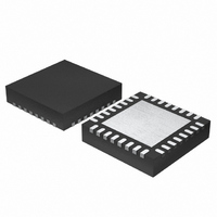
IC REG DUAL LNBP TTL-INP 32-QFN
Manufacturer
Intersil
Datasheet
1.ISL6424ERZ.pdf
(12 pages)
Specifications of ISL6424ERZ
Applications
Converter, Satellite Set-Top Box Designs
Voltage - Input
8 ~ 14 V
Number Of Outputs
2
Voltage - Output
13 ~ 18 V
Operating Temperature
-20°C ~ 85°C
Mounting Type
Surface Mount
Package / Case
32-VQFN Exposed Pad, 32-HVQFN, 32-SQFN, 32-DHVQFN
Lead Free Status / RoHS Status
Lead free / RoHS Compliant


Typical Performance Curves
Functional Pin Description
SEL18V1, 2 When connected HIGH, this pin will change the output
CPSWOUT
DSQIN1, 2 When HIGH enables internal 22kHz modulation for
PGND1, 2 Dedicated ground for the output gate driver of
COMP1, 2 Error amp outputs used for compensation.
SYMBOL
TCAP1, 2 Capacitor for setting rise and fall time of the output of
GATE1, 2 These are the device outputs of PWM A and PWM B
CPVOUT,
CPSWIN,
VSW1, 2
BYPASS
VO1, 2
CS1, 2
FB1, 2
SGND
AGND
ADDR
SDA
VCC
SCL
Bidirectional data from/to I
Clock from I
Input of the linear post-regulator.
respective PWM.
Current sense input; connect Rsc at this pin for
desired over current value for respective PWM.
Small signal ground for the IC.
Analog ground for the IC.
LNB A and LNB B respectively. Use this capacitor
value 1µF or higher.
Bypass capacitor for internal 5V.
LNB A and LNA B respectively, Use this pin for tone
enable function for LNB A and LNB B.
Main power supply to the chip.
respectively. These high current driver outputs are
capable of driving the gate of a power FET. These
outputs are actively held low when Vcc is below the
UVLO threshold.
Output voltage of LNB A and LNB B respectively.
Address pin to select two different addresses per
voltage level at this pin.
Feedback pins for respective PWMs
Charge pump connections.
of the respective PWM to 18V.
2
C bus.
7
FUNCTION
NOTE: With both channels in simultaneous operation at rated output
2
C bus.
0.80
0.70
0.60
0.50
0.40
0.30
0.20
0.10
0.00
0
FIGURE 1. OUTPUT CURRENT DERATING
20
ISL6424
TEMPERATURE (°C)
40
Functional Description
The ISL6424 dual output voltage regulator makes an ideal
choice for advanced satellite set-top box and personal video
recorder applications. Both supply and control voltage
outputs for two low-noise blocks (LNBs) are available
simultaneously in any output configuration. The device
utilizes built-in DC/DC step-converters that, from a single
supply source ranging from 8V to 14V, generate the voltages
that enable the linear post-regulators to work with a
minimum of dissipated power. An undervoltage lockout
circuit disables the circuit when VCC drops below a fixed
threshold (7.5V typ).
DiSEqC Encoding
The internal oscillator is factory-trimmed to provide a tone of
22kHz in accordance with DiSEqC (EUTELSAT) standards.
No further adjustment is required. The 22kHz oscillator can be
controlled either by the I
dedicated pin (DSQIN1/2) that allows immediate DiSEqC data
encoding separately for each LNB. (Please see Note 1 at the
end of this section.) All the functions of this IC are controlled
via the I
The same registers can be read back, and two bits will report
the diagnostic status. The internal oscillator operates the
converters at ten times the tone frequency. The device offers
full I
operation.
If the Tone Enable (ENT1/2) bit is set LOW through I
the DSQIN1/2 terminal activates the internal tone signal,
modulating the dc output with a 0.3V, 22kHz, symmetrical
waveform. The presence of this signal usually gives the LNB
information about the band to be received.
Burst coding of the 22kHz tone can be accomplished due to
the fast response of the DSQIN1/2 input and rapid tone
response. This allows implementation of the DiSEqC
(EUTELSAT) protocols.
2
C compatible functionality, 3.3V or 5V, and up to 400kHz
2
C bus by writing to the system registers (SR1, SR2).
60
I
OUT
_max
80
2
C interface (ENT1/2 bit) or by a
September 13, 2005
2
C, then
FN9175.3
Related parts for ISL6424ERZ
Image
Part Number
Description
Manufacturer
Datasheet
Request
R

Part Number:
Description:
Single Output LNB Supply and Control Voltage Regulator
Manufacturer:
Intersil
Datasheet:

Part Number:
Description:
Intersil Corporation [CMOS Serial Controller Interface]
Manufacturer:
Intersil Corporation
Datasheet:
Part Number:
Description:
Manufacturer:
Intersil Corporation
Datasheet:
Part Number:
Description:
357-036-542-201 CARDEDGE 36POS DL .156 BLK LOPRO
Manufacturer:
Intersil Corporation
Datasheet:
Part Number:
Description:
1024-Word x 4-Bit LSI Static RAM
Manufacturer:
Intersil Corporation
Datasheet:
Part Number:
Description:
General Purpose NPN Transistor Arrays FN341.4
Manufacturer:
Intersil Corporation
Datasheet:
Part Number:
Description:
CMOS 16-Bit Microprocessor
Manufacturer:
Intersil Corporation
Datasheet:
Part Number:
Description:
Manufacturer:
Intersil Corporation
Datasheet:
Part Number:
Description:
Manufacturer:
Intersil Corporation
Datasheet:
Part Number:
Description:
Manufacturer:
Intersil Corporation
Datasheet:
Part Number:
Description:
Manufacturer:
Intersil Corporation
Datasheet:
Part Number:
Description:
CMOS 6-Bit Latch and Decoder Memory Interfaces
Manufacturer:
Intersil Corporation
Datasheet:
Part Number:
Description:
CA3046General Purpose NPN Transistor Arrays
Manufacturer:
Intersil Corporation
Datasheet:
Part Number:
Description:
Manufacturer:
Intersil Corporation
Datasheet:
Part Number:
Description:
TR909 DLC/FLC SLIC with Low Power Standby
Manufacturer:
Intersil Corporation
Datasheet: