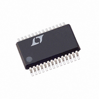
LTC1703IG#TR Linear Technology, LTC1703IG#TR Datasheet - Page 23

LTC1703IG#TR
Manufacturer Part Number
LTC1703IG#TR
Description
IC CTLR REG SW DUAL 2PH 28-SSOP
Manufacturer
Linear Technology
Datasheet
1.LTC1703CG.pdf
(36 pages)
Specifications of LTC1703IG#TR
Applications
Controller, Mobile Intel Pentium® III
Voltage - Input
3 ~ 7 V
Number Of Outputs
2
Voltage - Output
0.9 ~ 2 V
Operating Temperature
-40°C ~ 85°C
Mounting Type
Surface Mount
Package / Case
28-SSOP
Lead Free Status / RoHS Status
Contains lead / RoHS non-compliant
APPLICATIO S I FOR ATIO
If breadboard measurement is not practical, a SPICE
simulation can be used to generate approximate gain/
phase curves. Plug the expected capacitor, inductor and
MOSFET values into the following SPICE deck and gener-
ate an AC plot of V(V
ANALYZER
accurate results, but simulation can often get close enough
to give a working system. To measure the modulator gain
and phase directly, wire up a breadboard with an LTC1703
and the actual MOSFETs, inductor, and input and output
capacitors that the final design will use. This breadboard
should use appropriate construction techniques for high
speed analog circuitry: bypass capacitors located close to
the LTC1703, no long wires connecting components,
appropriately sized ground returns, etc. Wire the feedback
amplifier as a simple type 1 loop, with a 10k resistor from
V
FB. Choose the bias resistor (R
desired output voltage. Disconnect R
connect it to a signal generator or to the source output of
a network analyzer (Figure 12) to inject a test signal into the
loop. Measure the gain and phase from the COMP pin to
the output node at the positive terminal of the output
capacitor. Make sure the analyzer’s input is AC coupled so
that the DC voltages present at both the COMP and V
nodes don’t corrupt the measurements or damage the
analyzer.
ANALYZER
OUT
SOURCE
V
FROM
COMP
Figure 12. Modulator Gain/Phase Measurement Set-Up
TO
AC
to FB and a 0.1µF feedback capacitor from COMP to
10µF
0.1µF
R
+
B
10k
NC
COMP
FB
RUN/SS
SGND PGND
U
V
1/2 LTC1703
CC
OUT
10Ω
BOOST2
PV
FAULT
)/V(COMP) in dB and phase of
U
CC
FCB
SW
MBR0530T
TG
BG
B
) as required to set the
5V
W
QT
QB
+
B
1703 F12
from ground and
1µF
C
IN
L
EXT
+
U
C
V
TO
ANALYZER
OUT
OUT
OUT
V(OUT) in degrees. Refer to your SPICE manual for details
of how to generate this plot.
*1703 modulator gain/phase
*
*this file written to run with PSpice 8.0
*may require modifications for other SPICE
simulators
*MOSFETs
rfet mod sw 0.02
*inductor
lext sw out1 1u
rl out1 out 0.005
*output cap
cout out out2 1000u
resr out2 0 0.01
*1703 internals
emod mod 0 laplace {v(comp)} =
+ {5*exp(–s*909e–9)} ;5 -> 3.3 for 3.3 VCC
*emod mod 0 comp 0 5
vstim comp 0 0 ac 1
.ac dec 100 1k 1meg
.probe
.end
With the gain/phase plot in hand, a loop crossover fre-
quency can be chosen. Usually the curves look something
like Figure 8. Choose the crossover frequency in the rising
or flat parts of the phase curve, beyond the external LC
poles. Frequencies between 10kHz and 50kHz usually
work well. Note the gain (GAIN, in dB) and phase (PHASE,
in degrees) at this point. The desired feedback amplifier
gain will be – GAIN to make the loop gain 0dB at this
frequency. Now calculate the needed phase boost, assum-
ing 60° as a target phase margin:
If the required BOOST is less than 60°, a type 2 loop can
be used successfully, saving two external components.
BOOST values greater than 60° usually require type 3
loops for satisfactory performance.
Finally, choose a convenient resistor value for R1 (10k is
usually a good value). Note that channel 1 includes R1 and
R
at 10kΩ and R
selected.
©
B
1999 Linear Technology
BOOST = – (PHASE + 30°)
internally as part of the VID DAC circuitry. R1 is fixed
B
varies depending on the VID code
;MOSFET rdson
;inductor value
;inductor series R
;capacitor value
;capacitor ESR
;use if above lines fail
;ac stimulus
LTC1703
23
1703fa


