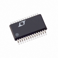
LTC1703IG#TR Linear Technology, LTC1703IG#TR Datasheet - Page 15

LTC1703IG#TR
Manufacturer Part Number
LTC1703IG#TR
Description
IC CTLR REG SW DUAL 2PH 28-SSOP
Manufacturer
Linear Technology
Datasheet
1.LTC1703CG.pdf
(36 pages)
Specifications of LTC1703IG#TR
Applications
Controller, Mobile Intel Pentium® III
Voltage - Input
3 ~ 7 V
Number Of Outputs
2
Voltage - Output
0.9 ~ 2 V
Operating Temperature
-40°C ~ 85°C
Mounting Type
Surface Mount
Package / Case
28-SSOP
Lead Free Status / RoHS Status
Contains lead / RoHS non-compliant
APPLICATIO S I FOR ATIO
Burst Mode Operation
Discontinuous mode removes a loss term due to resistive
drop in QB, but the LTC1703 is still switching QT and QB
on and off once a cycle. Each time an external MOSFET is
turned on, the internal driver must charge its gate to V
Each time it is turned off, that charge is lost to ground. At
the high switching frequencies that the LTC1703 operates
at, the charge lost to the gates can add up to tens of
milliamps from V
this quickly become the dominant power loss term, reduc-
ing efficiency once again.
Once again, the LTC1703 switches to a new mode to
minimize efficiency loss: Burst Mode operation. As the
circuit goes deeper and deeper into discontinuous mode,
the total time QT and QB are on reduces. However, the ratio
of the time that QT is on to the time that QB is on must
remain constant for the output to stay in regulation. An
internal timer circuit forces QT to stay on for at least 10%
of a normal switching cycle. When the load drops to the
point that the output requires less than 10% on-time at QT,
the output voltage will begin to rise. The LTC1703 senses
this rise and shuts both QT and QB off completely, skip-
ping several switching cycles until the output falls back
into range. It then resumes switching in discontinuous
mode with QT at 10% duty cycle and the burst sequence
repeats. The total deviation from the regulated output is
within the 1.5% regulation tolerance of the LTC1703.
In Burst Mode operation, both resistive loss and switching
loss are minimized while keeping the output in regulation.
The ripple current will be set by the 10% QT on-time and
the input supply voltage and is the lowest of all three
operating modes. As the load current falls to zero in Burst
Mode operation, the most significant loss term becomes
the 3mA quiescent current drawn by each side of the
LTC1703—usually much less than the minimum load
current in a typical low voltage logic system. Burst Mode
operation maximizes efficiency at low load currents, but
can cause low frequency ripple in the output voltage as the
cycle-skipping circuitry switches on and off.
FCB Pin
In some circumstances, it is desirable to control or disable
discontinuous and Burst Mode operations. The FCB (Force
CC
. As the load current continues to drop,
U
U
W
U
CC
.
Continuous Bar) pin allows the user to do this. When the
FCB pin is high, the LTC1703 is allowed to enter discon-
tinuous and Burst Mode operations at either side as
required. If FCB is taken low, discontinuous and Burst
Mode operations are disabled and both sides of the
LTC1703 run in continuous mode regardless of load. This
does not affect output regulation but does reduce effi-
ciency at low output currents. The FCB pin threshold is
specified at 0.8V ±50mV, and includes 20mV of hyster-
esis, allowing it to be used as a precision small-signal
comparator.
Paralleling Outputs
Synchronous regulators (like the LTC1703) are known for
their bullheadedness when their outputs are paralleled
with other regulators. In particular, a synchronous regu-
lator paralleled with another regulator whose output is
slightly higher (perhaps just by millivolts) will happily sink
amps of current attempting to pull its own output back
down to what it thinks is the right value.
The LTC1703 discontinuous mode allows it to be paral-
leled with another regulator without fighting. A typical
system might use the LTC1703 as a primary regulator and
a small LDO as a backup regulator to keep SRAM alive
when the main power is off. When the LTC1703 is shut
down (by pulling RUN/SS to ground), both QT and QB turn
off and the output goes into a high impedance state,
allowing the smaller regulator to support the output volt-
age. However, if the LTC1703 is powered back up in
continuous mode, it will begin a soft-start cycle with a low
duty cycle, pulling the output down and corrupting the
data stored in SRAM. The solution is to tie FCB high,
allowing the device to start in discontinuous mode. Any
reverse current flow in QB will trip the discontinuous mode
circuitry, preventing the LTC1703 from pulling down the
output.
OVERVOLTAGE FAULT
The LTC1703 includes a single overvoltage fault flag for
both channels: FAULT. FAULT is an open-drain output
with an internal 10µA pull-up. If either FB pin rises more
than 15% above the nominal 800mV value for more than
25µs, the overvoltage comparator will trip, setting an
LTC1703
15
1703fa


