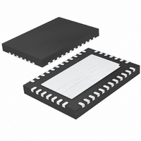
LTC3738CUHF Linear Technology, LTC3738CUHF Datasheet - Page 8

LTC3738CUHF
Manufacturer Part Number
LTC3738CUHF
Description
IC CTRLR SW REG 3PH STPDWN 38QFN
Manufacturer
Linear Technology
Datasheet
1.LTC3738CUHF.pdf
(32 pages)
Specifications of LTC3738CUHF
Applications
Controller, Intel VRM9, VRM10
Voltage - Input
3.8 ~ 36 V
Number Of Outputs
1
Voltage - Output
0.84 ~ 1.6 V
Operating Temperature
0°C ~ 85°C
Mounting Type
Surface Mount
Package / Case
38-QFN
Lead Free Status / RoHS Status
Contains lead / RoHS non-compliant
Available stocks
Company
Part Number
Manufacturer
Quantity
Price
Company:
Part Number:
LTC3738CUHF
Manufacturer:
LT
Quantity:
10 000
Part Number:
LTC3738CUHF
Manufacturer:
LINEAR/凌特
Quantity:
20 000
LTC3738
FCB/SYNC (Pin 1): Forced Continuous Control Input. The
voltage applied to this pin sets the operating mode of the
controller. The forced continuous current mode is active
when the applied voltage is less than 0.6V. Pulse skip
mode operation will be active when the pin is allowed to
float and Stage Shedding mode will be active if the pin is
tied to the V
controller will be synchronized to the external clock and
forced continuous mode is selected internally. (Do not
apply voltage to this pin prior to the application of voltage
on the V
PLLFLTR (Pin 2): The phase-locked loop’s lowpass filter
is tied to this pin. Alternatively, this pin can be driven with
an AC or DC voltage source to vary the frequency of the
internal oscillator. (Do not apply voltage to this pin prior to
the application of voltage on the V
IN
Differential Amplifier with Internal Precision Resistors.
This provides true remote sensing of both the positive and
negative load terminals for precise output voltage control.
AVP (Pin 5): Active Voltage Positioning Load Slope Pro-
gramming Pin. A resistor tied between this pin and IN
sets the load slope.
EAIN (Pin 6): This is the input to the error amplifier which
compares the VID divided feedback voltage to the internal
0.6V reference voltage.
SENSE1
SENSE3
Current Comparator. The I
offsets between the SENSE
tion with R
PI FU CTIO S
8
+
U
, IN
–
+
–
CC
(Pins 4, 3): Inputs to a Precision, Unity-Gain
, SENSE2
(Pins 7 to 12): The Inputs to Each Differential
U
SENSE
pin.)
CC
pin. When an external clock is present, the
, set the current trip threshold level.
+
U
, SENSE3
–
and SENSE
TH
+
pin voltage and built-in
, SENSE1
CC
pin.)
+
pins, in conjunc-
–
, SENSE2
–
+
,
SS (Pin 13): Combination of Soft-Start and Short-Circuit
Detection Timer. A capacitor to ground at this pin sets the
ramp time to full current output as well as the time delay
prior to an output voltage short-circuit shutdown.
I
lator Compensation Point. All three current comparator’s
thresholds increase with this control voltage.
TSNS (Pin 15): This pin selects external or internal ther-
mal detection. Tying this pin to V
thermal detector. When the voltage at this pin is less than
V
this pin serves as the input to an internal comparator
which is referenced to V
VR_HOTB (Pin 16): This open-collector output is pulled
low when voltage at the TSNS pin is less than V
TSNS is tied to V
thermal detector is tripped.
PGND (Pin 24): Driver Power Ground. This pin connects
to the sources of the bottom N-channel external MOSFETs
and the (–) terminals of C
BG1, BG2, BG3 (Pins 25, 23, 22): High Current Gate
Drives for the Bottom N-Channel MOSFETs. Voltage swing
at these pins is from ground to V
V
both the controller circuit power as well as the high power
pulses supplied to drive the external MOSFET gates, this
pin needs to be very carefully and closely decoupled to the
IC’s PGND pin.
TH
CC
CC
(Pin 14): Error Amplifier Output and Switching Regu-
– 1.6V, the internal thermal detector is disabled and
(Pin 26): Main Supply Pin. Because this pin supplies
CC
, this pin is pulled low when the internal
CC
IN
/3.
.
CC
CC
will enable the internal
.
CC
/3. If
3738f


