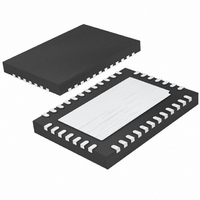
LTC3738CUHF Linear Technology, LTC3738CUHF Datasheet - Page 17

LTC3738CUHF
Manufacturer Part Number
LTC3738CUHF
Description
IC CTRLR SW REG 3PH STPDWN 38QFN
Manufacturer
Linear Technology
Datasheet
1.LTC3738CUHF.pdf
(32 pages)
Specifications of LTC3738CUHF
Applications
Controller, Intel VRM9, VRM10
Voltage - Input
3.8 ~ 36 V
Number Of Outputs
1
Voltage - Output
0.84 ~ 1.6 V
Operating Temperature
0°C ~ 85°C
Mounting Type
Surface Mount
Package / Case
38-QFN
Lead Free Status / RoHS Status
Contains lead / RoHS non-compliant
Available stocks
Company
Part Number
Manufacturer
Quantity
Price
Company:
Part Number:
LTC3738CUHF
Manufacturer:
LT
Quantity:
10 000
Part Number:
LTC3738CUHF
Manufacturer:
LINEAR/凌特
Quantity:
20 000
APPLICATIO S I FOR ATIO
The Schottky diodes shown in the Typical Application on
the first page of this data sheet conduct during the dead
time between the conduction of the two large power
MOSFETs. This prevents the body diode of the bottom
MOSFET from turning on, storing charge during the dead
time and requiring a reverse recovery period which could
cost as much as several percent in efficiency. A 2A to 8A
Schottky is generally a good compromise for both regions
of operation due to the relatively small average current.
Larger diodes result in additional transition losses due to
their larger junction capacitance.
C
Input capacitance ESR requirements and efficiency losses
are reduced substantially in a multiphase architecture
because the peak current drawn from the input capacitor
is effectively divided by the number of phases used and
power loss is proportional to the RMS current squared. A
3-stage, single output voltage implementation can reduce
input path power loss by 90%.
In continuous mode, the source current of each top
N-channel MOSFET is a square wave of duty cycle V
A low ESR input capacitor sized for the maximum RMS
current must be used. The details of a close form equation
can be found in Application Note 77. Figure 5 shows the
input capacitor ripple current for different phase configu-
rations with the output voltage fixed and input voltage
varied. The input ripple current is normalized against the
DC output current. The graph can be used in place of
tedious calculations. The minimum input ripple current
can be achieved when the product of phase number and
output voltage, N(V
input voltage V
So the phase number can be chosen to minimize the input
capacitor size for the given input and output voltages.
In the graph of Figure 5, the local maximum input RMS
capacitor currents are reached when:
IN
V
V
and C
V
V
OUT
OUT
IN
IN
=
=
OUT
N
2
k
k
N
Selection
where k
–
IN
1
or:
where k
U
OUT
= 1 2
), is approximately equal to the
U
, , ..., –
=
1 2
, , ...,
N
W
1
N
U
OUT
/V
IN
.
These worst-case conditions are commonly used for de-
sign because even significant deviations do not offer much
relief. Note that capacitor manufacturer’s ripple current
ratings are often based on only 2000 hours of life. This
makes it advisable to further derate the capacitor or to
choose a capacitor rated at a higher temperature than re-
quired. Several capacitors may also be paralleled to meet
size or height requirements in the design. Always consult
the capacitor manufacturer if there is any question.
The Figure 5 graph shows that the peak RMS input current
is reduced linearly, inversely proportional to the number N
of stages used. It is important to note that the efficiency
loss is proportional to the input RMS current squared and
therefore a 3-stage implementation results in 90% less
power loss when compared to a single phase design. Bat-
tery/input protection fuse resistance (if used), PC board
trace and connector resistance losses are also reduced by
the reduction of the input ripple current in a PolyPhase
system. The required amount of input capacitance is
further reduced by the factor, N, due to the effective in-
crease in the frequency of the current pulses.
Ceramic capacitors are becoming very popular for small
designs but several cautions should be observed. “X7R”,
“X5R” and “Y5V” are examples of a few of the ceramic
materials used as the dielectric layer, and these different
dielectrics have very different effect on the capacitance
value due to the voltage and temperature conditions
Figure 5. Normalized Input RMS Ripple Current
vs Duty Factor for One to Six Output Stages
0.6
0.5
0.4
0.3
0.2
0.1
0
0.1
0.2
0.3
DUTY FACTOR (V
0.4
1-PHASE
2-PHASE
3-PHASE
4-PHASE
6-PHASE
0.5
OUT
0.6
/V
IN
0.7
)
0.8
3738 F05
LTC3738
0.9
17
3738f


