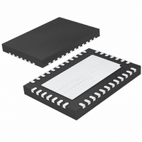
LT3513IUHF#PBF Linear Technology, LT3513IUHF#PBF Datasheet

LT3513IUHF#PBF
Specifications of LT3513IUHF#PBF
Available stocks
Related parts for LT3513IUHF#PBF
LT3513IUHF#PBF Summary of contents
Page 1
... L, LT, LTC, LTM, Linear Technology and the Linear logo are registered trademarks and PanelProtect, True Color PWM and ThinSOT are trademarks of Linear Technology Corporation. All other trademarks are the property of their respective owners. ...
Page 2
... LEAD FREE FINISH TAPE AND REEL LT3513EUHF#PBF LT3513EUHF#TRPBF LT3513IUHF#PBF LT3513IUHF#TRPBF Consult LTC Marketing for parts specified with wider operating temperature ranges. *The temperature grade is identified by a label on the shipping container. For more information on lead free part marking, go to: For more information on tape and reel specifications, go to: ...
Page 3
T PARAMETER FB Threshold Offset to Begin C Charge T C Pin Current Source T C Threshold to Power Switch Drop ON Maximum V Current ON V Input ...
Page 4
LT3513 elecTrical characTerisTics temperature range, otherwise specifications are at T PARAMETER Switch 3 (250mA BOOST) FB3 Voltage FB3 Voltage Line Regulation FB3 Pin Bias Current Error Amplifier 3 Voltage Gain Error Amplifier 3 Transconductance Switch 3 Current Limit Switch 3 ...
Page 5
Typical perFormance characTerisTics Maximum Output Current for V = 3.3V LOGIC 2.6 2 4.3µH 2 2.4µH 2.0 1.8 1.6 1.4 1 (V) IN 3513 G01 BOOST Pin Current ...
Page 6
LT3513 Typical perFormance characTerisTics SW3 V CESAT 300 250 200 150 100 50 0 200 300 350 0 50 100 150 250 I (mA) SW3 3513 G10 Oscillator Frequency 2.5 2.4 2.3 2.2 2.1 2.0 1.9 1.8 1.7 50 –50 ...
Page 7
Typical perFormance characTerisTics BIAS Pin Current 10µ 10µ 10µ SW2 SW3 SW4 10 0 – 100 150 TEMPERATURE ...
Page 8
LT3513 pin FuncTions FB5 (Pin 1): Feedback Pin. Tie the resistor tap to this pin and set the output of the LDO according R14/R15). Reference designators refer to Figure 1. V (Pin 2): Control Voltage and ...
Page 9
FuncTions V (Pin 20): Control Voltage and Compensation Pin for C2 Internal Error Amplifier. Connect a series RC from this pin to ground to compensate switching regulator 2. V (Pin 21): Control Voltage and Compensation Pin for C4 Internal ...
Page 10
LT3513 block Diagram LDOPWR FB5 36,37 INTERNAL RUN-SS1 22 REGULATOR AND REFERENCE FB1 32 PGOOD 11 FB2 19 20µ 1.25V UVLO – 38 3.9µA 2µA RUN-SS3/4 SW3 3 LOCKOUT 2µA ...
Page 11
The LT3513 is a highly integrated power supply IC contain- ing four separate switching regulators and a low dropout linear regulator (LDO). Switching regulator step- down 2.2A regulator with inductor current sense and an integrated boost ...
Page 12
LT3513 operaTion A power good comparator monitors AV when FB2 above 90% of its regulated value. The output is an open-collector transistor that is off when the output is out of regulation, allowing an external resistor to ...
Page 13
This leads to a minimum input voltage of OUT IN(MIN) Dc – MAX F SW with DC = 0.75. MAX The user defined undervoltage is set ...
Page 14
LT3513 operaTion The current in the inductor is a triangle wave with an average value equal to the load current. The peak switch current is equal to the output current plus half the peak-to-peak inductor ripple current. The LT3513 limits ...
Page 15
The low ESR and small size of ceramic capacitors make them the preferred type for LT3513 applications. However, not all ceramic capacitors are the same. Many of the higher value capacitors use poor dielectrics with high temperature and voltage ...
Page 16
LT3513 operaTion output. The minimum load current generally goes to zero once the circuit has started. Even without an output load current, in many cases the discharged output capacitor will present a load to the switcher that will allow it ...
Page 17
Output Capacitor Selection Use low ESR (equivalent series resistance) capacitors at the output to minimize the output ripple voltage. Multilayer ceramic capacitors are an excellent choice, as they have an extremely low ESR and are available in very small ...
Page 18
LT3513 operaTion below the rated voltage of the capacitor. Be sure to place the 1µF ceramic as close as possible to the V pins on the IC for optimal noise immunity. A final caution is in order regarding the use ...
Page 19
The loop formed by the components in the switched current path should be as small as possible. Place these components, along ...
Page 20
LT3513 package DescripTion 5.50 ± 0.05 4.10 ± 0.05 3.00 REF APPLY SOLDER MASK TO AREAS THAT ARE NOT SOLDERED 5.00 ± 0.10 PIN 1 TOP MARK (SEE NOTE 6) 7.00 ± 0.10 NOTE: 1. DRAWING CONFORMS TO JEDEC PACKAGE ...
Page 21
... Revised UVLO Pin Hysteresis Current and Switch 2 Current Limit Max values in Electrical Characteristics section Information furnished by Linear Technology corporation is believed to be accurate and reliable. However, no responsibility is assumed for its use. Linear Technology corporation makes no represen- tation that the interconnection of its circuits as described herein will not infringe on existing patent rights. ...
Page 22
... OUT(MAX 40V 65µA, I < 1µA, OUT(MAX 32V 6mA, I < 12µA, OUT(MAX 32V 1.65mA, I < 9µA, OUT(MAX 40V 4mA, I < 9µA, OUT(MAX 3,000:1 True Color PWM, I < 3µ 0111 REV C • PRINTED IN USA LINEAR TECHNOLOGY CORPORA TION 2008 3513fc ...


