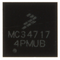
MC34717EP Freescale Semiconductor, MC34717EP Datasheet - Page 15

MC34717EP
Manufacturer Part Number
MC34717EP
Description
IC CONVERTER DDR 26QFN
Manufacturer
Freescale Semiconductor
Datasheet
1.MC34717EP.pdf
(28 pages)
Specifications of MC34717EP
Applications
Converter, DDR
Voltage - Input
3 ~ 6 V
Number Of Outputs
2
Voltage - Output
0.7 ~ 3.6 V
Operating Temperature
-40°C ~ 85°C
Mounting Type
Surface Mount
Package / Case
26-QFN
Output Voltage
0.7 V to 3.6 V
Output Current
5 A
Input Voltage
3 V to 6 V
Switching Frequency
1 MHz
Operating Temperature Range
- 40 C to + 85 C
Mounting Style
SMD/SMT
No. Of Outputs
2
Power Dissipation Pd
2.03W
No. Of Pins
26
Filter Terminals
SMD
Rohs Compliant
Yes
Lead Free Status / RoHS Status
Lead free / RoHS Compliant
Available stocks
Company
Part Number
Manufacturer
Quantity
Price
Part Number:
MC34717EP
Manufacturer:
FREESCALE
Quantity:
20 000
TRACKING AND SEQUENCING
the voltage applied at the VREFIN pin in different tracking
configurations. This will be discussed in further details later in
this document. For power down during a shutdown mode, the
34717 uses internal discharge MOSFETs (M8 and M9 on
Figure
respectively. The discharge MOSFETs are only active during
shutdown mode. Using this block along with controlling the
SD pin can offer the user power sequencing capabilities by
controlling when to turn the 34717 outputs on or off.
BUCK CONVERTER
DC conversion from an un-regulated input voltage to a
regulated output voltage used by the loads for reliable
operation. The buck converter is a high performance, fixed
Analog Integrated Circuit Device Data
Freescale Semiconductor
This block allows the second output of the 34717 to track
This block provides the main function of the 34717: DC to
2, page 2) to discharge the first and second output
frequency (externally adjustable), synchronous buck PWM
voltage-mode control. It drives integrated 50m
power MOSFETs saving board space and enhancing
efficiency. The switching regulator output voltage is
adjustable with an accuracy of less than ±2% to meet today’s
requirements. The second channel’s output has the ability to
track the voltage applied at the VREFIN pin. The regulator's
voltage control loop is compensated using a type III
compensation network, with external components to allow for
optimizing the loop compensation, for a wide range of
operating conditions. A typical Bootstrap circuit with an
internal PMOS switch is used to provide the voltage
necessary to properly enhance the high side MOSFET gate.
continuous current from each channel, making it suitable for
many high current applications.
The 34717 has the ability to supply up to 5.0 A of
FUNCTIONAL INTERNAL BLOCK DESCRIPTION
FUNCTIONAL DESCRIPTION
Ω
N-channel
34717
15


