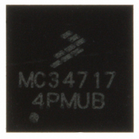
MC34717EP Freescale Semiconductor, MC34717EP Datasheet - Page 12

MC34717EP
Manufacturer Part Number
MC34717EP
Description
IC CONVERTER DDR 26QFN
Manufacturer
Freescale Semiconductor
Datasheet
1.MC34717EP.pdf
(28 pages)
Specifications of MC34717EP
Applications
Converter, DDR
Voltage - Input
3 ~ 6 V
Number Of Outputs
2
Voltage - Output
0.7 ~ 3.6 V
Operating Temperature
-40°C ~ 85°C
Mounting Type
Surface Mount
Package / Case
26-QFN
Output Voltage
0.7 V to 3.6 V
Output Current
5 A
Input Voltage
3 V to 6 V
Switching Frequency
1 MHz
Operating Temperature Range
- 40 C to + 85 C
Mounting Style
SMD/SMT
No. Of Outputs
2
Power Dissipation Pd
2.03W
No. Of Pins
26
Filter Terminals
SMD
Rohs Compliant
Yes
Lead Free Status / RoHS Status
Lead free / RoHS Compliant
Available stocks
Company
Part Number
Manufacturer
Quantity
Price
Part Number:
MC34717EP
Manufacturer:
FREESCALE
Quantity:
20 000
more efficient and accurate power supplies. They present a
set of challenges that include highly accurate voltage
regulation, high current and fast transient response
capability, voltage monitoring (power sequencing), and
increased operating frequency. Point of Load power supplies
offer adequate solutions to these challenges. They are non-
isolated DC to DC converters that are located near their load
and take their input voltage from an intermediate not,
necessarily, regulated bus. their close proximity to the load is
of a high importance with newer device requirements. While
meeting the challenges, they allow for higher efficiency,
localized protection, and minimum distribution losses. Their
compact design and value makes them cost effective.
integrated solution offers a cost effective system and reliable
operation. It utilizes a voltage mode synchronous buck
switching converter topology with integrated low R
(50 mΩ) N-channel power MOSFETs for higher efficiency
operation. It provides an output voltage with an accuracy of
less than
BOOTSTRAP INPUT (BOOT1, BOOT2)
discussed in
pin and the SW pin of the respective channel to enhance the
gate of the high side Power MOSFET during switching.
POWER INPUT VOLTAGE (PVIN1, PVIN2)
buck converter high side power MOSFET.
SWITCHING NODE (SW1, SW2)
the output inductor.
POWER GROUND (PGND1, PGND2)
is the source of the buck converter low side power MOSFET.
COMPENSATION INPUT (COMP1, COMP2)
to this pin. Use a type III compensation network.
ERROR AMPLIFIER INVERTING INPUT (INV1, INV2)
V
12
34717
FUNCTIONAL DESCRIPTION
INTRODUCTION
DDQ
Today’s advanced systems are increasingly requiring
The 34717 is a PoL dual output power supply. Its
Bootstrap capacitor input pin. Connect a capacitor (as
Buck converter power input voltage. This is the drain of the
Buck converter switching node. This pin is connected to
Buck converter and discharge MOSFETs power ground. It
Buck converter external compensation network connects
Buck converter error amplifier inverting input. Connect the
voltage (channel 1) to INV1 pin through a resistor
±
2.0%, and capable of supplying up to 5.0 A of
Bootstrap capacitor on page
21) between this
FUNCTIONAL DESCRIPTION
FUNCTIONAL PIN DESCRIPTION
DS(ON)
INTRODUCTION
continuous current from both channels. The second output
tracking abilities makes it ideal for systems with multiple
related supply rails. It has a programmable switching
frequency that allows for flexibility and optimization over the
operating conditions and can operate at up to 1.0 MHz to
significantly reduce the external components size and cost. It
also provides the ability to program the over current limit for
both channels. It protects against output over-current, over-
voltage, under-voltage, and over-temperature conditions. It
also protects the system from short circuit events. It
incorporates a power good output signal to alert the host
when a fault occurs.
which offers power sequencing capabilities.
the Power MOSFET switches for the buck converter into a
space-efficient package, the 34717 offers a complete, small-
size, cost-effective, and simple solution to satisfy the needs
of today’s systems.
divider and connect the V
INV2 pin.
INTERNAL SUPPLY VOLTAGE OUTPUT (VDDI)
Connect a 1.0 µF, 6.0 V low ESR ceramic filter capacitor
between this pin and the GND pin. Filtering any spikes on this
output is essential to the internal circuitry stable operation.
SIGNAL GROUND (GND)
referenced to this pin voltage.
INPUT SUPPLY VOLTAGE (VIN)
the device to operate properly.
POWER GOOD OUTPUT SIGNAL (PG)
report the status of the device to a host. This output activates
after a successful power up sequence and stays active as
long as the device is in normal operation and is not
experiencing any faults. This output activates after a 10 ms
delay and must be pulled up by an external resistor to a
supply voltage like V
It can be enabled and disabled by controlling the SD pin,
By integrating the control/supervisory circuitry along with
This is the output of the internal bias voltage regulator.
Analog ground of the IC. Internal analog signals are
IC power supply input voltage. Input filtering is required for
This is an active low open drain output that is used to
IN
.
Analog Integrated Circuit Device Data
TT
voltage (channel 2) directly to
Freescale Semiconductor


