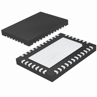
LT3513EUHF#PBF Linear Technology, LT3513EUHF#PBF Datasheet - Page 9

LT3513EUHF#PBF
Manufacturer Part Number
LT3513EUHF#PBF
Description
IC REG 5-OUT FOR TFT-LCD 38QFN
Manufacturer
Linear Technology
Datasheet
1.LT3513EUHFPBF.pdf
(22 pages)
Specifications of LT3513EUHF#PBF
Applications
Converter, TFT, LCD
Voltage - Input
4.5 ~ 30 V
Number Of Outputs
5
Voltage - Output
0.8 ~ 40 V
Operating Temperature
-40°C ~ 125°C
Mounting Type
Surface Mount
Package / Case
38-QFN
Lead Free Status / RoHS Status
Lead free / RoHS Compliant
Available stocks
Company
Part Number
Manufacturer
Quantity
Price
pin FuncTions
V
Internal Error Amplifier. Connect a series RC from this pin
to ground to compensate switching regulator 2.
V
Internal Error Amplifier. Connect a series RC from this pin
to ground to compensate switching regulator 4.
RUN-SS1 (Pin 22): Run/Soft-Start Pin. This is the soft-start
pin for switching regulator 1. Place a soft-start capacitor
here to limit start-up inrush current and output voltage
ramp rate. When power is applied to the V
current source charges the capacitor. When the voltage
at this pin reaches 0.8V, switch 1 turns on and begins
switching. For slower start-up use a larger capacitor. For
complete shutdown tie RUN-SS1 to ground.
NFB4 (Pin 23): Negative Feedback Pin. Tie the resistor di-
vider tap to this pin and set V
(1 + R3/R4). Reference designators refer to Figure 2.
D4 (Pin 24): Internal Schottky Diode Pin. This pin is the
anode of an internal Schottky diode with the other end
connected to ground. This Schottky diode is used in
generating the V
SW4 (Pin 25): Switch Node. The SW4 pin is the collector of
the internal NPN bipolar transistor for switching regulator 4.
Minimize trace area at this pin to keep EMI down.
BD (Note 26): NPN LDO Base Drive. This pin controls the
base of the external NPN LDO transistor.
LDOPWR (Pin 27): Input Voltage for LDO Driver. This pin
supplies the current for the NPN LDO base. This pin can
be connected to V
the pin can alternatively be connected to the AV
BOOST (Pin 28): The BOOST pin is used to provide a
drive voltage higher than V
An internal Schottky diode is connected between BIAS
and BOOST. A capacitor needs to be connected between
BOOST and SW1.
C2
C4
(Pin 20): Control Voltage and Compensation Pin for
(Pin 21): Control Voltage and Compensation Pin for
OFF
IN
. To save power at high V
output.
IN
OFF
to the switch 1 drive circuit.
according to V
IN
OFF
IN
pin, a 2µA
DD
voltages,
= –1.18 •
supply.
SENSE
(along with the SENSE
current for the buck switching regulator.
SENSE
(along with the SENSE
current for the buck switching regulator.
FB1 (Pin 32): Feedback Pin. Tie the resistor divider tap
to this pin and set V
(1 + R1/R2). Reference designators refer to Figure 2.
SW1 (Pins 34, 35): Switch Node. The SW1 pins are the
emitter of the internal NPN bipolar power transistor for
switching regulator 1. These points must be tied together
for proper operation. Connect these pins to the inductor,
catch diode and boost capacitor.
V
to the internal circuitry of the LT3513. This pin must be
locally bypassed with a capacitor.
UVLO (Pin 38): Undervoltage Lockout. A resistor divider
connected to V
input voltage at which the LT3513 will operate. This pin is
compared to the internal 1.25V reference. When UVLO is
less than 1.25V, the switching regulators are not allowed
to operate (the RUN/SS pins are still used to turn on each
switching regulator). When this pin falls below 1.25V,
3.9µA will be pulled from the pin to provide programmable
hysteresis for UVLO.
Exposed Pad (Pin 39): Ground. The Exposed Pad of the
package provides both electrical contact to ground and
good thermal contact to the printed circuit board. The
Exposed Pad must be soldered to the circuit board for
proper operation.
IN
(Pins 36, 37): Input Voltage. This pin supplies current
–
+
(Pin 30) Negative Current Sense Input. This pin
(Pin 31) Positive Current Sense Input. This pin
IN
is tied to this pin to program the minimum
LOGIC
+
–
pin) is used to sense the inductor
pin) is used to sense the inductor
according to V
LOGIC
LT3513
= 1.235V •
3513fc
9


