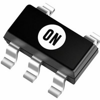
NCP1550SN25T1 ON Semiconductor, NCP1550SN25T1 Datasheet - Page 2

NCP1550SN25T1
Manufacturer Part Number
NCP1550SN25T1
Description
IC CTR PFM/PWM DCDC 2.5V TSOT235
Manufacturer
ON Semiconductor
Datasheet
1.NCP1550SN18T1.pdf
(17 pages)
Specifications of NCP1550SN25T1
Pwm Type
Voltage Mode
Number Of Outputs
1
Frequency - Max
690kHz
Duty Cycle
100%
Voltage - Supply
2.45 V ~ 5.5 V
Buck
Yes
Boost
No
Flyback
No
Inverting
No
Doubler
No
Divider
No
Cuk
No
Isolated
No
Operating Temperature
-40°C ~ 85°C
Package / Case
TSOT-23-5, TSOT-5, TSOP-5
Frequency-max
690kHz
Mounting Style
SMD/SMT
Lead Free Status / RoHS Status
Contains lead / RoHS non-compliant
Other names
NCP1550SN25T1OSTR
Available stocks
Company
Part Number
Manufacturer
Quantity
Price
Part Number:
NCP1550SN25T1G
Manufacturer:
ON/安森美
Quantity:
20 000
Stresses exceeding Maximum Ratings may damage the device. Maximum Ratings are stress ratings only. Functional operation above the
Recommended Operating Conditions is not implied. Extended exposure to stresses above the Recommended Operating Conditions may affect
device reliability.
NOTE:
1. This device series contains ESD protection and exceeds the following tests:
2. Latchup Current Maximum Rating: 150 mA per JEDEC standard: JESD78.
3. Moisture Sensitivity Level (MSL): 1 per IPC/JEDEC standard: J−STD−020A.
PIN FUNCTION DESCRIPTIONS
MAXIMUM RATINGS
Pin
Device Power Supply, V
Input/Output Pins
Thermal Characteristics
Operating Junction Temperature Range
Operating Ambient Temperature Range
Storage Temperature Range
1
2
3
4
5
CE (Pin 1)
V
EXT (Pin 4)
TSOP−5 Plastic Package, Case 483−01
Thermal Resistance, Junction−to−Air
OUT
Machine Model (MM) $200V per JEDEC standard: JESD22−A115.
Human Body Model (HBM) $2.0 kV per JEDEC standard: JESD22−A114.
Symbol
(Pin 3)
ESD data available upon request.
V
GND
EXT
V
CE
OUT
IN
V
GND
OUT
Chip Enable pin, active high (internal pullup current source). By connecting this pin to GND, the switching operation
of the controller will be stopped.
Ground Connection
Output voltage monitoring input. This pin must be connected to the regulated output node as a feedback to on−chip
control circuitry. V
Gate drive for external P−MOSFET
Power supply input
(T
IN
3
2
A
(Pin 5)
= 25°C unless otherwise noted)
M1
OUT
Rating
is internally connected to the on−chip voltage divider that determines the output voltage level.
Figure 1. Simplified Block Diagram
A1
−
+
Voltage Reference
and Soft−Start
http://onsemi.com
T
Controller
T
ON(PFM)
NCP1550
PWM
ON
t
2
Description
Oscillator
600 kHz
CP1
2.2 V + −
+
−
Symbol
Driver
V
V
R
V
T
UVLO
V
T
OUT
T
EXT
qJA
stg
CE
IN
A
J
−40 to +150
−55 to +150
−0.3 to 6.0
−0.3 to 6.0
−0.3 to 6.0
−0.3 to 6.0
−40 to +85
5
4
1
Value
250
V
EXT
CE
IN
°C/W
Unit
°C
°C
°C
V
V


