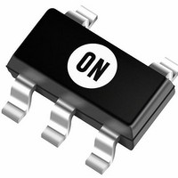
NCP1550SN25T1 ON Semiconductor, NCP1550SN25T1 Datasheet

NCP1550SN25T1
Specifications of NCP1550SN25T1
Available stocks
Related parts for NCP1550SN25T1
NCP1550SN25T1 Summary of contents
Page 1
NCP1550 600 kHz PWM/PFM Step−Down DC−DC Controller The NCP1550 is a monolithic micropower high frequency voltage mode step−down controller IC, specially designed for battery operated hand−held electronic products. With appropriate external P−type MOSFET, the device can provide up to 2.0 ...
Page 2
V OUT 2 GND M1 PIN FUNCTION DESCRIPTIONS Pin Symbol 1 CE Chip Enable pin, active high (internal pullup current source). By connecting this pin to GND, the switching operation of the controller will be stopped. 2 GND Ground ...
Page 3
... NCP1550SN19T1 NCP1550SN25T1 NCP1550SN27T1 NCP1550SN30T1 NCP1550SN33T1 Off−State Current ( NCP1550SN18T1 NCP1550SN19T1 NCP1550SN25T1 NCP1550SN27T1 NCP1550SN30T1 NCP1550SN33T1 OSCILLATOR Frequency Frequency Temperature Coefficient (T = −40°C to 85°C) A Maximum Duty Cycle PWM/PFM Switchover ON Time Threshold (Note 4) Soft−Start Delay Time (Note 4) Protection Delay Time (Auto Restart) OUTPUT DRIVE (PIN 4) EXT “ ...
Page 4
ELECTRICAL CHARACTERISTICS unless otherwise noted.) Characteristic CE (PIN 1) CE “H” Input Voltage CE “L” Input Voltage CE “H” Input Current ( 5 “L” Input Current ( ...
Page 5
... Figure 5. Efficiency versus Load Current NCP1550 100 1000 1 I LOAD Figure 4. Efficiency versus Load Current 4 3 5.0 V NCP1550SN18T1 OUT M = NTGS3441T1 SD = MBRM120LT3 10 100 I , OUTPUT LOADING CURRENT (mA) LOAD http://onsemi.com 5 = 3.0 V 4.0 V 5.0 V NCP1550SN25T1 OUT M = NTGS3441T1 SD = MBRM120LT3 10 100 , OUTPUT LOADING CURRENT (mA) 1000 1000 ...
Page 6
TYPICAL OPERATING CHARACTERISTICS OUT M = NTGS3441T1 0 MBRM120LT3 1 −0.3 2.7 V −0.6 −0.9 10 100 I , OUTPUT ...
Page 7
L = 3 LOAD Upper Trace: Output Voltage Ripple, 50 mV/Division Middle Trace: Inductor Current 500 mA/Division L Lower Trace: Voltage at Cathode of Schottky Diode, 2.0 ...
Page 8
L = 5 LOAD Upper Trace: Output Voltage Ripple, 50 mV/Division Middle Trace: Inductor Current 500 mA/Division L Lower Trace: Voltage at Cathode of Schottky Diode, 2.0 ...
Page 9
L = 6 LOAD Upper Trace: Output Voltage Ripple, 50 mV/Division Middle Trace: Inductor Current 500 mA/Division L Lower Trace: Voltage at Cathode of Schottky Diode, 2.0 ...
Page 10
3 OUT Upper Trace: Output Voltage Ripple, 100 mV/Division Lower Trace: Input Voltage, 2.0 V/Division Figure 23. Line Transient Response for V = 3.3 V ...
Page 11
5 LOAD = 33 mF) C OUT Upper Trace: Output Voltage Ripple, 100 mV/Division Lower Trace: Load Current 500 mA/Division LOAD Figure 27. ...
Page 12
... Figure 37. NCP1550 EXT “L” Output Current versus Ambient Temperature NCP1550 2.55 2.53 2.51 2.49 = 5.0 V 2.47 2. 100 −50 −25 Figure 34. NCP1550SN25T1 Output Voltage −40 −50 −60 −70 −80 = 5.0 V −90 −100 50 75 100 −50 −25 Figure 36. NCP1550 EXT “H” Output Current 3 ...
Page 13
Detailed Operating Description The NCP1550 series are step−down (Buck) DC−DC controllers designed primarily for use in portable applications powered by battery cells. With an appropriate external P−channel MOSFET connected, the device can provide loading current with ...
Page 14
Inductor Value Calculation Selecting the proper inductance is a trade−off between inductor’s physical size, transient respond and power conversion requirements. Lower value inductor saves cost, PC board space and providing faster transient response, but result in higher ripple current and ...
Page 15
... External Component Reference Data Device V Inductor Model OUT NCP1550SN18T1 1.8 V CDD5D23 CDRH6D38 6R8 (2A) Sumida NCP1550SN19T1 1.9 V CDC5D23 CDRH6D38 6R8 (2A) Sumida NCP1550SN25T1 2.5 V CDC5D23 CDRH6D38 5R0 (2A) Sumida NCP1550SN27T1 2.7 V CDC5D23 CDRH6D38 5R0 (2A) Sumida NCP1550SN30T1 3.0 V CDC5D23 CDRH6D28 5R0 (2A) Sumida NCP1550SN33T1 3 ...
Page 16
... V NCP1550SN30T1 3.0 V NCP1550SN30T1G 3.0 V NCP1550SN27T1 2.7 V NCP1550SN27T1G 2.7 V NCP1550SN25T1 2.5 V NCP1550SN25T1G 2.5 V NCP1550SN19T1 1.9 V NCP1550SN19T1G 1.9 V NCP1550SN18T1 1.8 V NCP1550SN18T1G 1.8 V †For information on tape and reel specifications, including part orientation and tape sizes, please refer to our Tape and Reel Packaging Specifications Brochure, BRD8011/D. ...
Page 17
... H T *For additional information on our Pb−Free strategy and soldering details, please download the ON Semiconductor Soldering and Mounting Techniques Reference Manual, SOLDERRM/D. ON Semiconductor and are registered trademarks of Semiconductor Components Industries, LLC (SCILLC). SCILLC reserves the right to make changes without further notice to any products herein. SCILLC makes no warranty, representation or guarantee regarding the suitability of its products for any particular purpose, nor does SCILLC assume any liability arising out of the application or use of any product or circuit, and specifically disclaims any and all liability, including without limitation special, consequential or incidental damages. “ ...


