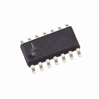
HIP6013CB-T Intersil, HIP6013CB-T Datasheet - Page 4

HIP6013CB-T
Manufacturer Part Number
HIP6013CB-T
Description
IC CONTROLLER PWM BUCK 14-SOIC
Manufacturer
Intersil
Datasheet
1.HIP6013CBZ.pdf
(11 pages)
Specifications of HIP6013CB-T
Pwm Type
Voltage Mode
Number Of Outputs
1
Frequency - Max
1MHz
Duty Cycle
100%
Voltage - Supply
2.5 V ~ 12 V
Buck
Yes
Boost
No
Flyback
No
Inverting
No
Doubler
No
Divider
No
Cuk
No
Isolated
No
Operating Temperature
0°C ~ 70°C
Package / Case
14-SOIC (3.9mm Width), 14-SOL
Frequency-max
1MHz
Lead Free Status / RoHS Status
Contains lead / RoHS non-compliant
Available stocks
Company
Part Number
Manufacturer
Quantity
Price
Company:
Part Number:
HIP6013CB-T
Manufacturer:
SWREG
Quantity:
646
Part Number:
HIP6013CB-T
Manufacturer:
INTERSIL
Quantity:
20 000
Typical Performance Curves
Functional Pin Description
RT (Pin 1)
This pin provides oscillator switching frequency adjustment.
By placing a resistor (R
200kHz switching frequency is increased according to the
following equation:
Conversely, connecting a pull-up resistor (R
VCC reduces the switching frequency according to the
following equation.:
OCSET (Pin 2)
Connect a resistor (R
upper MOSFET. R
(I
the converter over-current (OC) trip point according to the
following equation:
An over-current trip cycles the soft-start function.
Fs
I
Fs
PEAK
OCS
≈
≈
1000
200kHz
200kHz
100
), and the upper MOSFET on-resistance (r
10
=
10
FIGURE 1. R
I
------------------------------------------- -
OCS
–
+
r
DS ON
OCSET
4 10
------------------
5 10
------------------
•
COMP
•
R
•
R
(
GND
R
OCSET
T
EN
RT
SS
FB
T
OCSET
7
6
)
SWITCHING FREQUENCY (kHz)
T
OCSET
1
2
3
4
5
6
7
RESISTANCE vs FREQUENCY
T
) from this pin to GND, the nominal
(R
, an internal 200µA current source
R
(R
T
T
T
PULLUP
TO +12V
) from this pin to the drain of the
to 12V)
R
to GND)
4
T
100
PULLDOWN
TO V
14
13
12
11
10
9
8
SS
VCC
NC
NC
BOOT
UGATE
PHASE
NC
T
) from this pin to
DS(ON)
1000
) set
HIP6013
SS (Pin 3)
Connect a capacitor from this pin to ground. This capacitor,
along with an internal 10µA current source, sets the soft-
start interval of the converter.
COMP (Pin 4) and FB (Pin 5)
COMP and FB are the available external pins of the error
amplifier. The FB pin is the inverting input of the error
amplifier and the COMP pin is the error amplifier output.
These pins are used to compensate the voltage-control
feedback loop of the converter.
EN (Pin 6)
This pin is the open-collector enable pin. Pull this pin below
1V to disable the converter. In shutdown, the soft start pin is
discharged and the UGATE and LGATE pins are held low.
GND (Pin 7)
Signal ground for the IC. All voltage levels are measured with
respect to this pin.
PHASE (Pin 8)
Connect the PHASE pin to the upper MOSFET source. This
pin is used to monitor the voltage drop across the MOSFET
for over-current protection. This pin also provides the return
path for the upper gate drive.
UGATE (Pin 9)
Connect UGATE to the upper MOSFET gate. This pin
provides the gate drive for the upper MOSFET.
BOOT (Pin 10)
This pin provides bias voltage to the upper MOSFET driver.
A bootstrap circuit may be used to create a BOOT voltage
suitable to drive a standard N-Channel MOSFET.
VCC (Pin 14)
Provide a 12V bias supply for the chip to this pin.
40
35
30
25
20
15
10
FIGURE 2. BIAS SUPPLY CURRENT vs FREQUENCY
5
0
100
200
300
SWITCHING FREQUENCY (kHz)
400
C
GATE
500
C
= 3300pF
C
GATE
GATE
600
= 1000pF
= 10pF
700
800
November 3, 2005
900
1000
4325.1


