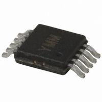
MIC3839BMM TR Micrel Inc, MIC3839BMM TR Datasheet - Page 9

MIC3839BMM TR
Manufacturer Part Number
MIC3839BMM TR
Description
IC CTRLR DC/DC PUSH-PULL 10-MSOP
Manufacturer
Micrel Inc
Datasheet
1.MIC3839YMM.pdf
(11 pages)
Specifications of MIC3839BMM TR
Pwm Type
Voltage/Current Mode
Number Of Outputs
1
Frequency - Max
1MHz
Duty Cycle
50%
Voltage - Supply
2 V ~ 14 V
Buck
Yes
Boost
No
Flyback
No
Inverting
No
Doubler
No
Divider
No
Cuk
No
Isolated
Yes
Operating Temperature
-40°C ~ 85°C
Package / Case
10-MSOP, Micro10™, 10-uMAX, 10-uSOP
Frequency-max
1MHz
Lead Free Status / RoHS Status
Contains lead / RoHS non-compliant
Other names
MIC3839BMMTR
MIC3839BMMTR
MIC3839BMMTR
Soft Start
The soft start feature helps reduce surge currents at the
power supply input source. An internal current source and
capacitor ramp up from 0V to near V
1V/ms. The soft start feature limits the output voltage of the
error amplifier at the COMP pin. As the soft start voltage rises,
it allows the COMP pin voltage to rise, which in turn allows the
duty cycle of the output drivers to increase. The internal soft
start voltage is discharged and remains discharged during
the following conditions:
Once the internal soft start discharge FET is turned on, it
cannot be turned off until the internal soft start voltage drops
down below 0.5V. This insures a clean restart.
Oscillator
The oscillator operates at twice the switching frequency of
either OUTA or OUTB. The oscillator generates a sawtooth
waveform on the RC pin. The rising edge of the waveform is
controlled by the external resistor/capacitor combination.
The fall time is set by the on-resistance of the discharge FET
(see Figure 3). The fall time sets the delay (dead time)
between the turn-off of one output driver and the turn-on of the
other driver. A toggle flip-flop insures that drive signals to
OUTA and OUTB are alternated and therefore insures a
maximum duty cycle of less than 50% for each output driver.
Graphs of component values vs. oscillator frequency and
dead time are shown in the typical characteristic section of
this specification.
The voltage source to the resistor/capacitor timing compo-
nents is V
oscillator circuit is V
changes in V
oscillator. The oscillator frequency can be roughly approxi-
mated using the following formula:
Where: frequency is in Hz
April 2005
MIC3838/3839
1. The V
2. The voltage on the CS pin exceeds the overcur-
F
threshold.
rent comparator threshold.
OSCILLATOR
V
Resistance is in ohms
Capacitance is in Farads.
DD
DD
RC
. The internal turn-off comparator threshold in the
DD
4
DD
voltage drops below the turn-off
and minimize frequency variations in the
VDD
0.2V
2
Figure 3. Oscillator
=
DD
R C
1.41
/2. This allows the oscillator to track
×
S
R
Q
DD
at a typical rate of
OSCILLATOR
OUTPUT
9
Graphs of oscillator frequency and dead time vs component
values are shown in the Typical Characteristic section of this
specification. The recommended range of timing resistors
and capacitors is 7kΩ to 200kΩ and 100pF to 1000pF. To
minimize oscillator noise and insure a stable waveform the
following layout rules should be followed:
Current Sensing and Overcurrent Protection
The features are:
In current mode control, a PWM comparator uses the inductor
current signal and the error amplifier signal to determine the
operating duty cycle. In the MIC3838/9 the signal at the CS
pin is level shifted up before it reaches the PWM comparator
as shown in Figure 1. This allows operation of the error
amplifier and PWM comparator in a linear region.
There are two current limit thresholds in the MIC3838/9; peak
current limit and overcurrent limit. The normal operating
voltage at the I
A pulse-by-pulse current limit occurs when the inductor
current signal at the I
threshold. The on-time is terminated for the remainder of the
switching cycle, regardless of whether OUTA or OUTB is
active.
If the signal at the I
exceeds the overcurrent limit threshold, the overcurrent limit
comparator forces the soft start node to discharge and
initiates a soft start reset.
An internal FET discharges the RAMP and I
of the oscillator charge time. The FET turns on when the
voltage on the RC pin reaches the upper threshold (V
and remains on for the duration of the RC pin discharge time
and for typically 100ns after the start of the next on-time
period. The 100ns period at the beginning of the on-time
implements a front edge blanking feature that prevents false
triggering of the PWM comparator due to noise spikes on the
leading edge of the current turn-on signal. The front edge
blanking also sets the minimum on-time for OUTA and OUTB.
The timing diagram for the RAMP pin is shown in Figure 4.
1. The higher impedance of capacitor values less
2. The circuit board etch between the timing
3. The ground lead of the capacitor must be routed
• Peak current limit
• Overcurrent limit
• Internal current sense discharge
• Front edge blanking
than 100pF may causes the oscillator circuit to
become more susceptible to noise. Parasitic pin
and etch trace capacitances become a larger
part of the total RC capacitance and may
influence the desired switching frequency.
resistor, capacitor, RC pin and ground must be
kept as short as possible to minimize noise
pickup and insure a stable oscillator waveform.
close to the ground lead of the MIC3838/9.
LIM
pin is designed less than these thresholds.
LIM
LIM
pin goes past the peak threshold and
pin exceeds the peak current limit
LIM
MIC3838/3839
pins at the end
Micrel
DD
/2)


