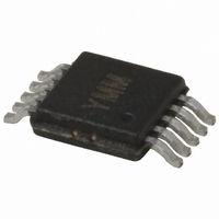
MIC3839BMM TR Micrel Inc, MIC3839BMM TR Datasheet - Page 10

MIC3839BMM TR
Manufacturer Part Number
MIC3839BMM TR
Description
IC CTRLR DC/DC PUSH-PULL 10-MSOP
Manufacturer
Micrel Inc
Datasheet
1.MIC3839YMM.pdf
(11 pages)
Specifications of MIC3839BMM TR
Pwm Type
Voltage/Current Mode
Number Of Outputs
1
Frequency - Max
1MHz
Duty Cycle
50%
Voltage - Supply
2 V ~ 14 V
Buck
Yes
Boost
No
Flyback
No
Inverting
No
Doubler
No
Divider
No
Cuk
No
Isolated
Yes
Operating Temperature
-40°C ~ 85°C
Package / Case
10-MSOP, Micro10™, 10-uMAX, 10-uSOP
Frequency-max
1MHz
Lead Free Status / RoHS Status
Contains lead / RoHS non-compliant
Other names
MIC3839BMMTR
MIC3839BMMTR
MIC3839BMMTR
MIC3838/3839
Error Amplifier
The error amplifier is part of the voltage control loop of the
power supply. The FB pin is the inverting input to the error
amplifier. The non-inverting input is internally connected to a
reference voltage. The output of the error amplifier, COMP,
is connected to the PWM comparator. A voltage divider
between the error amplifier output (COMP pin) and the PWM
comparator allows the error amplifier to operate in a linear
region for better transient response. The output of the error
amplifier (COMP pin) is clamped at typically 3.65V to prevent
the COMP pin from rising up too high during startup or during
a transient condition. This feature improves the transient
response of the power supply.
MIC3838/3839
Oscillator
AMP Pin
OUTB
OUTA
C Pin
eset
Figure 4. Timing Diagram
Max ON
time
dead time
dead time
Front edge blanking
Minimum ON time
10
Output Drivers
OUTA and OUTB are alternating output stages, which switch
at half the oscillator frequency. A toggle flip-flop in the
MIC3838/9 guarantee both outputs will not be on at the same
time. The RC discharge time is the dead time, where both
outputs are off. This provides an adjustable non-overlap time
to prevent shoot through currents and transformer saturation
in the power supply.
The output drivers are inhibited when V
undervoltage threshold. Internal circuitry prevents the output
drivers from glitching high when V
MIC3838/9 controller.
Decoupling and PCB Layout
PCB layout is critical to achieve reliable, stable and efficient
operation. A ground plane is required to control EMI and
minimize the inductance in power, signal and return paths.
The following guidelines should be followed to insure proper
operation of the circuit:
• Low level signal and power grounds should be kept
• Avoid running sensitive traces, such as the current
• If a current sense resistor is used, it’s ground end must
• A minimum 1µF bypass capacitor must be connected
separate and connected at only one location, preferably
the ground pin of the control IC. The ground signals for
the current sense, voltage feedback and oscillator
should be grouped together. The return signals for the
gate drives should be grouped together and a common
connection made at the ground pin of the controller. The
low level signals and their returns must be kept separate
from the high current and high voltage power section of
the power supply.
sense and voltage feedback signals next to or under
power components, such as the switching FETs and
transformer.
be located very close to the ground pin of the MIC3838/9
controller. Careful PCB layout is necessary to keep the
high current levels in the current sense resistor from
running over the low level signals in the controller.
directly between the V
MIC3838/9. An additional 0.1µF capacitor between the
V
the ground end of the oscillator capacitor may be
necessary if the resistor is a distance away from the
main 1µF bypass capacitor
DD
end of the oscillator frequency setting resistor and
DD
and GND pins of the
DD
is first applied to the
DD
is below the
April 2005
Micrel


