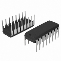
MC34025PG ON Semiconductor, MC34025PG Datasheet - Page 3

MC34025PG
Manufacturer Part Number
MC34025PG
Description
IC CTRLR PWM DBL END HF 16DIP
Manufacturer
ON Semiconductor
Specifications of MC34025PG
Pwm Type
Voltage/Current Mode
Number Of Outputs
2
Frequency - Max
1MHz
Duty Cycle
45%
Voltage - Supply
10 V ~ 30 V
Buck
No
Boost
No
Flyback
No
Inverting
No
Doubler
No
Divider
No
Cuk
No
Isolated
Yes
Operating Temperature
0°C ~ 70°C
Package / Case
16-DIP (0.300", 7.62mm)
Frequency-max
1MHz
Duty Cycle (max)
45 %
Output Voltage
5.05 V to 5.15 V
Output Current
500 mA
Mounting Style
Through Hole
Switching Frequency
1000 KHz
Operating Supply Voltage
30 V
Maximum Operating Temperature
+ 70 C
Fall Time
30 ns
Minimum Operating Temperature
0 C
Rise Time
30 ns
Synchronous Pin
Yes
Topology
Half-Bridge, Push-Pull
Number Of Pwm Outputs
2
On/off Pin
Yes
Adjustable Output
No
Switching Freq
1000kHz
Operating Supply Voltage (max)
30V
Operating Temperature Classification
Commercial
Mounting
Through Hole
Pin Count
16
Package Type
PDIP
Lead Free Status / RoHS Status
Lead free / RoHS Compliant
Other names
MC34025PGOS
Available stocks
Company
Part Number
Manufacturer
Quantity
Price
Part Number:
MC34025PG
Manufacturer:
ON/安森美
Quantity:
20 000
ELECTRICAL CHARACTERISTICS
T
ERROR AMPLIFIER SECTION
PWM COMPARATOR SECTION
SOFT−START SECTION
CURRENT SENSE SECTION
OUTPUT SECTION
UNDERVOLTAGE LOCKOUT SECTION
TOTAL DEVICE
3. Maximum package power dissipation limits must be observed.
4. Low duty cycle pulse techniques are used during test to maintain junction temperature as close to ambient as possible.
Input Offset Voltage
Input Bias Current
Input Offset Current
Open−Loop Voltage Gain (V
Gain Bandwidth Product (T
Common Mode Rejection Ratio (V
Power Supply Rejection Ratio (V
Output Current,
Output Voltage Swing,
Slew Rate
Ramp Input Bias Current
Duty Cycle of Each Output,
Zero Duty Cycle Threshold Voltage Pin 3(4) (Pin 7(9) = 0 V)
Propagation Delay (Ramp Input to Output, T
Charge Current (V
Discharge Current (V
Input Bias Current (Pin 9(12) = 0 V to 4.0 V)
Current Limit Comparator Threshold
Shutdown Comparator Threshold
Propagation Delay (Current Limit/Shutdown to Output, T
Output Voltage
Output Voltage with UVLO Activated (V
Output Leakage Current (V
Output Voltage Rise Time (C
Output Voltage Fall Time (C
Startup Threshold (V
UVLO Hysteresis Voltage (V
Power Supply Current
A
is the operating ambient temperature range that applies [Note 4], unless otherwise noted.)
T
T
Low State
High State
low
low
= 0°C for MC34025
= − 40°C for MC33025
Soft−Start
CC
Soft−Start
Increasing)
J
C
= 0.5 V)
Characteristic
L
O
CC
L
= + 25°C)
= 20 V)
= 1.0 nF, T
= 1.5 V)
= 1.0 V to 4.0 V)
= 1.0 nF, T
Decreasing After Turn−On)
CC
CM
= 10 V to 30 V)
T
T
= 1.5 V to 5.5 V)
high
high
CC
J
J
(V
= + 25°C)
= 6.0 V, I
= + 25°C)
= +70°C for MC34025
= +105°C for MC33025
CC
High State (I
J
= + 25°C)
Low State (I
= 15 V, R
Startup (V
Source (V
Sink
(I
Sink (V
(I
Source
(I
Source
(I
Sink
= 0.5 mA)
J
O
T
Sink
http://onsemi.com
= + 25°C)
= 3.65 kW, C
O
= − 0.5 mA)
CC
= 200 mA)
= 200 mA)
O
O
Operating
= 1.0 mA)
Maximum
= 20 mA)
= 20 mA)
Minimum
= 4.0 V)
= 1.0 V)
= 8.0 V)
3
T
= 1.0 nF, for typical values T
V
t
t
PLH(in/out)
PLH(in/out)
Symbol
DC
DC
OL(UVLO)
CMRR
PSRR
I
V
I
GBW
Source
A
dischg
I
V
V
V
V
I
V
SR
th(on)
I
Sink
V
V
V
V
I
I
VOL
I
chg
I
CC
I
IO
OH
(max)
OH
t
IB
OL
IB
(min)
IB
OL
t
IO
L
th
th
th
r
f
H
1.25
Min
4.0
0.5
1.0
4.5
6.0
1.1
3.0
1.0
0.9
8.8
0.4
60
75
85
40
13
12
−
−
−
0
−
−
−
−
−
−
−
−
−
−
−
−
−
A
= + 25°C, for min/max values
4.75
−0.5
1.25
1.40
0.25
13.5
0.25
Typ
100
110
0.6
0.1
8.3
3.0
3.6
0.4
9.0
4.0
1.0
1.2
9.2
0.8
0.5
95
95
12
45
60
50
13
30
30
25
−
−
−
−5.0
Max
1.10
1.55
100
500
3.0
1.0
5.0
1.0
1.4
0.4
2.2
1.0
9.6
1.2
1.2
15
20
15
80
60
60
35
−
−
−
−
−
−
−
−
0
−
−
−
MHz
Unit
V/ms
mV
mA
mA
mA
mA
mA
dB
dB
dB
mA
mA
mA
mA
ns
ns
ns
ns
%
V
V
V
V
V
V
V


