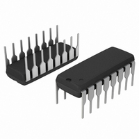
MC34025PG ON Semiconductor, MC34025PG Datasheet - Page 2

MC34025PG
Manufacturer Part Number
MC34025PG
Description
IC CTRLR PWM DBL END HF 16DIP
Manufacturer
ON Semiconductor
Specifications of MC34025PG
Pwm Type
Voltage/Current Mode
Number Of Outputs
2
Frequency - Max
1MHz
Duty Cycle
45%
Voltage - Supply
10 V ~ 30 V
Buck
No
Boost
No
Flyback
No
Inverting
No
Doubler
No
Divider
No
Cuk
No
Isolated
Yes
Operating Temperature
0°C ~ 70°C
Package / Case
16-DIP (0.300", 7.62mm)
Frequency-max
1MHz
Duty Cycle (max)
45 %
Output Voltage
5.05 V to 5.15 V
Output Current
500 mA
Mounting Style
Through Hole
Switching Frequency
1000 KHz
Operating Supply Voltage
30 V
Maximum Operating Temperature
+ 70 C
Fall Time
30 ns
Minimum Operating Temperature
0 C
Rise Time
30 ns
Synchronous Pin
Yes
Topology
Half-Bridge, Push-Pull
Number Of Pwm Outputs
2
On/off Pin
Yes
Adjustable Output
No
Switching Freq
1000kHz
Operating Supply Voltage (max)
30V
Operating Temperature Classification
Commercial
Mounting
Through Hole
Pin Count
16
Package Type
PDIP
Lead Free Status / RoHS Status
Lead free / RoHS Compliant
Other names
MC34025PGOS
Available stocks
Company
Part Number
Manufacturer
Quantity
Price
Part Number:
MC34025PG
Manufacturer:
ON/安森美
Quantity:
20 000
Stresses exceeding Maximum Ratings may damage the device. Maximum Ratings are stress ratings only. Functional operation above the
Recommended Operating Conditions is not implied. Extended exposure to stresses above the Recommended Operating Conditions may affect
device reliability.
1. Maximum package power dissipation limits must be observed.
2. Low duty cycle pulse techniques are used during test to maintain junction temperature as close to ambient as possible.
MAXIMUM RATINGS
ELECTRICAL CHARACTERISTICS
is the operating ambient temperature range that applies [Note 2], unless otherwise noted.)
REFERENCE SECTION
OSCILLATOR SECTION
Power Supply Voltage
Output Driver Supply Voltage
Output Current, Source or Sink (Note 1)
Current Sense, Soft−Start, Ramp, and Error Amp Inputs
Error Amp Output and Soft−Start Sink Current
Clock and R
Power Dissipation and Thermal Characteristics
Operating Junction Temperature
Operating Ambient Temperature (Note 2)
Storage Temperature Range
Reference Output Voltage (I
Line Regulation (V
Load Regulation (I
Temperature Stability
Total Output Variation over Line, Load, and Temperature
Output Noise Voltage (f = 10 Hz to 10 kHz, T
Long Term Stability (T
Output Short Circuit Current
Frequency
Frequency Change with Voltage (V
Frequency Change with Temperature (T
Sawtooth Peak Voltage
Sawtooth Valley Voltage
Clock Output Voltage
T
T
DC
Pulsed (0.5 ms)
SO−16 Package (Case 751G)
DIP Package (Case 648)
MC34025
MC33025
T
Line (V
High State
Low State
low
low
J
= + 25°C
Thermal Resistance, Junction−to−Air
= 0°C for MC34025
= − 40°C for MC33025
Maximum Power Dissipation @ T
Maximum Power Dissipation @ T
Thermal Resistance, Junction−to−Air
CC
T
= 10 V to 30 V) and Temperature (T
Output Current
CC
O
= 1.0 mA to 10 mA)
= 10 V to 30 V)
A
= +125°C for 1000 Hours)
Characteristic
O
= 1.0 mA, T
CC
T
T
Rating
high
high
= 10 V to 30 V)
A
A
A
= +70°C for MC34025
= +105°C for MC33025
(V
J
= T
= + 25°C
= + 25°C
= + 25°C)
CC
J
low
= + 25°C)
= 15 V, R
to T
A
= T
high
low
)
T
http://onsemi.com
to T
= 3.65 kW, C
high
)
2
T
= 1.0 nF, for typical values T
Df
Df
Symbol
Reg
Reg
osc
osc
V
V
V
V
f
I
T
V
V
V
osc
SC
S
OH
OL
ref
ref
S
n
P
V
load
line
/DV
/DT
Symbol
R
R
V
I
T
V
V
P
P
T
T
I
I
CO
qJA
qJA
CC
stg
O
O
5.05
4.95
in
A
C
D
D
Min
−30
380
370
J
2.6
0.7
3.9
−
−
−
−
−
−
−
−
A
= + 25°C, for min/max values T
Typ
−65
400
400
5.1
2.0
2.0
0.2
5.0
0.2
2.0
2.8
1.0
4.5
2.3
50
−
−0.3 to +7.0
−40 to +105
−55 to +150
0 to +70
Value
+150
1.25
862
145
100
0.5
2.0
5.0
30
25
10
−100
Max
5.15
5.25
1.25
420
430
1.0
3.0
2.9
15
15
−
−
−
−
−
°C/W
°C/W
mV/°C
Unit
mW
mA
mA
Unit
kHz
°C
°C
°C
W
mV
mV
mV
mA
V
V
A
V
mV
%
%
V
V
V
V
V
A


