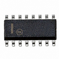
NCP1562ADR2G ON Semiconductor, NCP1562ADR2G Datasheet - Page 4

NCP1562ADR2G
Manufacturer Part Number
NCP1562ADR2G
Description
IC CLAMP/RESET PWM CTLR 16-SOIC
Manufacturer
ON Semiconductor
Datasheet
1.NCP1562ADBR2G.pdf
(26 pages)
Specifications of NCP1562ADR2G
Pwm Type
Voltage Mode
Number Of Outputs
2
Frequency - Max
1MHz
Duty Cycle
85%
Voltage - Supply
23.2 V ~ 100 V
Buck
No
Boost
Yes
Flyback
Yes
Inverting
Yes
Doubler
No
Divider
No
Cuk
No
Isolated
No
Operating Temperature
-40°C ~ 125°C
Package / Case
16-SOIC (3.9mm Width)
Frequency-max
1MHz
Topology
Flyback, Forward, Half-Bridge
Output Voltage
20 V
Output Current
2000 mA, 1000 mA
Switching Frequency
1000 KHz
Duty Cycle (max)
85 %
Maximum Operating Temperature
+ 125 C
Minimum Operating Temperature
- 40 C
Fall Time
10 ns
Mounting Style
SMD/SMT
Rise Time
26 ns
Synchronous Pin
Yes
Lead Free Status / RoHS Status
Lead free / RoHS Compliant
Other names
NCP1562ADR2G
NCP1562ADR2GOSTR
NCP1562ADR2GOSTR
Available stocks
Company
Part Number
Manufacturer
Quantity
Price
Company:
Part Number:
NCP1562ADR2G
Manufacturer:
ON Semiconductor
Quantity:
1 250
Part Number:
NCP1562ADR2G
Manufacturer:
ON/安森美
Quantity:
20 000
PIN FUNCTION DESCRIPTION
Pin
15
16
Symbol
OUT1
V
AUX
Main output of the PWM Controller. OUT1 has a source resistance of 4.0 Ω (typ.) and a sink resistance
of 2.5 Ω (typ.). OUT1 is designed to handle up to 2.5 A. OUT1 trails OUT2 during a low to high
transition and leads OUT2 during a high to low transition.
Positive input supply. This pin connects to an external capacitor for energy storage. An internal current
source supplies current from V
the current source turns OFF and the outputs are enabled. It turns ON again once V
the bias current consumption exceeds the startup current, V
reaches 7.0 V, the outputs are disabled allowing V
supplied to the IC via this pin by means of an auxiliary winding. The startup circuit is disabled once the
voltage on the V
current is reduced to 200 mA.
(continued)
AUX
pin exceeds 10.3 V. If the V
http://onsemi.com
in
4
to this pin. Once the voltage on V
Description
AUX
AUX
voltage drops below 1.2 V (typ), the startup
to charge. During normal operation, power is
AUX
will continue to discharge. Once V
AUX
reaches approximately 10.3 V,
AUX
falls to 8.0 V. If
AUX


