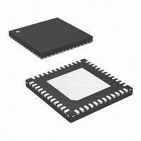
ISL6327IRZ-T Intersil, ISL6327IRZ-T Datasheet - Page 23

ISL6327IRZ-T
Manufacturer Part Number
ISL6327IRZ-T
Description
IC CTRLR PWM 6PHASE BUCK 48-QFN
Manufacturer
Intersil
Datasheet
1.ISL6327CRZ.pdf
(29 pages)
Specifications of ISL6327IRZ-T
Pwm Type
Voltage Mode
Number Of Outputs
1
Frequency - Max
275kHz
Duty Cycle
25%
Voltage - Supply
4.75 V ~ 5.25 V
Buck
Yes
Boost
No
Flyback
No
Inverting
No
Doubler
No
Divider
No
Cuk
No
Isolated
No
Operating Temperature
-40°C ~ 85°C
Package / Case
48-VQFN
Frequency-max
275kHz
Lead Free Status / RoHS Status
Lead free / RoHS Compliant
Available stocks
Company
Part Number
Manufacturer
Quantity
Price
Part Number:
ISL6327IRZ-T
Manufacturer:
INTERSIL
Quantity:
20 000
External Temperature Compensation
By pulling the TCOMP pin to GND, the integrated
temperature compensation function is disabled. And one
external temperature compensation network, shown in
Figure 16, can be used to cancel the temperature impact on
the droop (i.e. load line).
The sensed current will flow out of IDROOP pin and develop
the droop voltage across the resistor (R
VDIFF pins. If R
increases, the temperature impact on the droop can be
compensated. An NTC resistor can be placed close to the
power stage and used to form R
temperature characteristics of the NTC, a resistor network is
needed to make the equivalent resistance between FB and
VDIFF pin reverse proportional to the temperature.
The external temperature compensation network can only
compensate the temperature impact on the droop, while it
has no impact to the sensed current inside ISL6327.
Therefore, this network cannot compensate for the
temperature impact on the overcurrent protection function.
General Design Guide
This design guide is intended to provide a high-level
explanation of the steps necessary to create a multiphase
power converter. It is assumed that the reader is familiar with
many of the basic skills and techniques referenced below. In
addition to this guide, Intersil provides complete reference
designs that include schematics, bills of materials, and
example board layouts for all common microprocessor
applications.
Power Stages
The first step in designing a multiphase converter is to
determine the number of phases. This determination
depends heavily on the cost analysis which in turn depends
on system constraints that differ from one design to the next.
Principally, the designer will be concerned with whether
components can be mounted on both sides of the circuit
board; whether through-hole components are permitted; and
the total board space available for power-supply circuitry.
Generally speaking, the most economical solutions are
FIGURE 16. EXTERNAL TEMPERATURE COMPENSATION
FB
o
C
resistance reduces as the temperature
23
IDROOP
COMP
VDIFF
FB
FB
. Due to the non-linear
INTERNAL
FB
CIRCUIT
ISL6327
) between FB and
ISL6327
those in which each phase handles between 15A and 20A.
All surface-mount designs will tend toward the lower end of
this current range. If through-hole MOSFETs and inductors
can be used, higher per-phase currents are possible. In
cases where board space is the limiting constraint, current
can be pushed as high as 40A per phase, but these designs
require heat sinks and forced air to cool the MOSFETs,
inductors, and heat-dissipating surfaces.
MOSFETS
The choice of MOSFETs depends on the current each
MOSFET will be required to conduct; the switching
frequency; the capability of the MOSFETs to dissipate heat;
and the availability and nature of heat sinking and air flow.
LOWER MOSFET POWER CALCULATION
The calculation for heat dissipated in the lower MOSFET is
simple, since virtually all of the heat loss in the lower
MOSFET is due to current conducted through the channel
resistance (r
continuous output current; I
current (see Equation 1); d is the duty cycle (V
L is the per-channel inductance.
An additional term can be added to the lower-MOSFET loss
equation to account for additional loss accrued during the dead
time when inductor current is flowing through the lower
MOSFET body diode. This term is dependent on the diode
forward voltage at I
the length of dead times, t
end of the lower-MOSFET conduction interval respectively.
Thus the total maximum power dissipated in each lower
MOSFET is approximated by the summation of P
P
UPPER MOSFET POWER CALCULATION
In addition to r
MOSFET losses are due to currents conducted across the
input voltage (V
higher portion of the upper-MOSFET losses are dependent on
switching frequency, the power calculation is more complex.
Upper MOSFET losses can be divided into separate
components involving the upper-MOSFET switching times;
the lower-MOSFET body-diode reverse-recovery charge, Q
and the upper MOSFET r
When the upper MOSFET turns off, the lower MOSFET does
not conduct any portion of the inductor current until the
voltage at the phase node falls below ground. Once the
lower MOSFET begins conducting, the current in the upper
MOSFET falls to zero as the current in the lower MOSFET
P
P
LOW,2
LOW 1
LOW 2
,
,
.
=
=
r
V
DS ON
DS(ON)
D ON
(
DS(ON)
(
IN
) during switching. Since a substantially
)
)
M
f
S
). In Equation 24, I
⎛
⎜
⎝
, V
I
----- -
N
M
⎛
⎝
losses, a large portion of the upper
I
----- -
D(ON)
⎞
⎟
⎠
N
M
2
d1
DS(ON)
(
+
1 d
I
-------- -
P-P
–
PP
and t
2
; the switching frequency, f
⎞ t
⎠
)
+
is the peak-to-peak inductor
d1
d2
conduction loss.
I
--------------------------------
L PP
, at the beginning and the
,
+
2
⎛
⎜
⎝
12
I
----- -
M
(
N
M
1 d
is the maximum
–
–
I
-------- -
PP
2
)
⎞
⎟
⎠
OUT
t
d2
LOW,1
/V
May 5, 2008
IN
(EQ. 24)
(EQ. 25)
FN9276.4
S
); and
; and
and
rr
,


