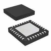
ISL9440BIRZ-T Intersil, ISL9440BIRZ-T Datasheet - Page 6

ISL9440BIRZ-T
Manufacturer Part Number
ISL9440BIRZ-T
Description
IC CTRLR PWM OUT-OF-PHASE 32-QFN
Manufacturer
Intersil
Datasheet
1.ISL9440BIRZ.pdf
(24 pages)
Specifications of ISL9440BIRZ-T
Pwm Type
Current Mode
Number Of Outputs
4
Frequency - Max
340kHz
Duty Cycle
93%
Voltage - Supply
4.5 V ~ 24 V
Buck
Yes
Boost
No
Flyback
No
Inverting
No
Doubler
No
Divider
No
Cuk
No
Isolated
No
Operating Temperature
-40°C ~ 85°C
Package / Case
32-VQFN Exposed Pad, 32-HVQFN, 32-SQFN, 32-DHVQFN
Frequency-max
340kHz
Lead Free Status / RoHS Status
Lead free / RoHS Compliant
Available stocks
Company
Part Number
Manufacturer
Quantity
Price
Company:
Part Number:
ISL9440BIRZ-T
Manufacturer:
Intersil
Quantity:
6 000
Absolute Maximum Ratings
VCC_5V to GND . . . . . . . . . . . . . . . . . . . . . . . . . . . . . . -0.3V to +6V
VCC_5V Output Current . . . . . . . . . . . . . . . . . . . . . . . . . . . . 100mA
VIN to GND . . . . . . . . . . . . . . . . . . . . . . . . . . . . . . . . . -0.3V to +28V
BOOT/UGATE to PHASE . . . . . . . . . . . . . -0.3V to VCC_5V + 0.3V
PHASE1,2,3 and ISEN1, 2, 3, to GND
EN/SS1,EN/SS2, EN/SS3, FB1, FB2,
LDOFB, OCSET1, OCSET2, OCSET3,
PGOOD, RST, G4 to GND . . . . . . . . . . . . . . . . . . . . . . . -0.3V to +6V
CAUTION: Do not operate at or near the maximum ratings listed for extended periods of time. Exposure to such conditions may adversely impact product reliability and
result in failures not covered by warranty.
NOTES:
Electrical Specifications
V
Input Voltage Range
Input Voltage Range
VCC_5V SUPPLY (Note 6)
Operation Voltage
Internal LDO Output Voltage
Maximum Supply Current of Internal LDO
V
Shutdown Current (Note 7)
Operating Current (Note 8)
REFERENCE SECTION
Internal Reference Voltage
Reference Voltage Accuracy
PWM CONTROLLER ERROR AMPLIFIERS
DC Gain (Note 9)
Gain-BW Product (Note 9)
Slew Rate (Note 9)
PWM REGULATOR
Switching Frequency (ISL9440B)
Maximum Duty Cycle (ISL9440B)
Minimum Duty Cycle (ISL9440B)
Switching Frequency (ISL9440C)
4. θ
5. For θ
FB3, to GND. . . . . . . . . . . . . . . . . . . . . . -0.3V to VCC_5V + 0.3V
LGATE1, LGATE2, LGATE3, to GND. . . -0.3V to VCC_5V + 0.3V
IN
IN
. . . . . . . . . . . . . . . . . . . . .-5V (<100ns, 10µJ)/-0.3V (DC) to +28V
Brief TB379.
SUPPLY
SUPPLY CURRENT
JA
is measured in free air with the component mounted on a high effective thermal conductivity test board with “direct attach” features. See Tech
JC
, the “case temp” location is the center of the exposed metal pad on the package underside.
PARAMETER
6
Recommended operating conditions unless otherwise noted. Refer to “Block Diagram” on page 3, “Typical
Application - ISL9440B” on page 4 and “Typical Application - ISL9440C” on page 5. V
VCC_5V = 5V ±10%, C_VCC_5V = 4.7µF, T
ISL9440B, ISL9440C
V
V
V
EN/SS1 = EN/SS2 = EN/SS3 = 0,
V
floating.
Across specified temperature range
Across specified temperature range
IN
IN
IN
IN
= VCC_5V (Note 10)
> 5.6V, I
= 12V
=12V. PGOOD and RST are
TEST CONDITIONS
Thermal Information
Thermal Resistance (Typical Notes 4, 5)
Maximum Junction Temperature . . . . . . . . . . . . . . .-55°C to +150°C
Maximum Operating Temperature . . . . . . . . . . . . . . .-40°C to +85°C
Maximum Storage Temperature. . . . . . . . . . . . . . . .-65°C to +150°C
Pb-Free Reflow Profile. . . . . . . . . . . . . . . . . . . . . . . . .see link below
A
L
32 Ld QFN Package. . . . . . . . . . . . . . .
http://www.intersil.com/pbfree/Pb-FreeReflow.asp
= 60mA
= -40°C to +85°C, Typical values are at T
(Note 11)
MIN
260
522
5.6
4.5
4.5
4.5
60
-1
TYP
12.0
5.0
5.0
5.0
0.8
2.0
300
600
IN
75
88
15
93
θ
3
3
JA
A
= 5.6V to 24V, or
= +25°C.
(°C/W)
31
(Note 11) UNITS
MAX
24.0
110
340
678
5.6
5.6
5.5
+1
5
June 24, 2010
θ
JC
(°C/W)
FN6799.3
2.3
MHz
V/µs
kHz
kHz
mA
mA
µA
dB
%
%
%
V
V
V
V
V


