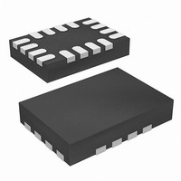
ISL62870HRUZ-T Intersil, ISL62870HRUZ-T Datasheet - Page 13

ISL62870HRUZ-T
Manufacturer Part Number
ISL62870HRUZ-T
Description
IC CTRLR VREG PWM DC/DC 16-TQFN
Manufacturer
Intersil
Datasheet
1.ISL62870HRUZ-T.pdf
(16 pages)
Specifications of ISL62870HRUZ-T
Pwm Type
Controller
Number Of Outputs
1
Frequency - Max
330kHz
Duty Cycle
100%
Voltage - Supply
3.3 V ~ 25 V
Buck
Yes
Boost
No
Flyback
No
Inverting
No
Doubler
No
Divider
No
Cuk
No
Isolated
No
Operating Temperature
-10°C ~ 100°C
Package / Case
16-UTQFN (16-µTQFN)
Frequency-max
330kHz
Lead Free Status / RoHS Status
Lead free / RoHS Compliant
Available stocks
Company
Part Number
Manufacturer
Quantity
Price
Company:
Part Number:
ISL62870HRUZ-T
Manufacturer:
M/A-COM
Quantity:
45
Part Number:
ISL62870HRUZ-T
Manufacturer:
INTERSIL
Quantity:
20 000
Where:
Layout Considerations
The IC, analog signals, and logic signals should all be on the
same side of the PCB, located away from powerful emission
sources. The power conversion components should be
arranged in a manner similar to the example in Figure 12
where the area enclosed by the current circulating through
the input capacitors, high-side MOSFETs, and low-side
MOSFETs is as small as possible and all located on the
same side of the PCB. The power components can be
located on either side of the PCB relative to the IC.
Signal Ground
The GND pin is the signal-common also known as analog
ground of the IC. When laying out the PCB, it is very
important that the connection of the GND pin to the bottom
feedback voltage-divider resistor and the C
be made as close as possible to the GND pin on a conductor
not shared by any other components.
In addition to the critical single point connection discussed in
the previous paragraph, the ground plane layer of the PCB
should have a single-point-connected island located under
the area encompassing the IC, feedback voltage divider,
compensation components, C
interconnecting traces among the components and the IC.
The island should be connected using several filled vias to
the rest of the ground plane layer at one point that is not in
the path of either large static currents or high di/dt currents.
The single connection point should also be where the VCC
decoupling capacitor and the GND pin of the IC are
connected.
- I
- I
- t
- t
FIGURE 12. TYPICAL POWER COMPONENT PLACEMENT
inductor current minus 1/2 of the inductor ripple current
current plus 1/2 of the inductor ripple current
saturation
VALLEY
PEAK
ON
OFF
HIGH-SIDE
MOSFETS
is the time required to drive the device into
is the time required to drive the device into cut-off
HIGH-SIDE
MOSFETS
is the sum of the DC component of the inductor
is the difference of the DC component of the
PHASE
NODE
VOUT
GND
+
PHASE
VOUT
NODE
GND
VIN
VIN
+
13
SOFT
OUTPUT
CAPACITORS
OUTPUT
CAPACITORS
capacitor, and the
LOW-SIDE
MOSFETS
INPUT
CAPACITORS
LOW-SIDE
MOSFETS
INPUT
CAPACITORS
SOFT
capacitor
ISL62870
Power Ground
Anywhere not within the analog-ground island is Power
Ground.
VCC AND PVCC PINS
Place the decoupling capacitors as close as practical to the
IC. In particular, the PVCC decoupling capacitor should have
a very short and wide connection to the PGND pin. The VCC
decoupling capacitor should not share any vias with the
PVCC decoupling capacitor.
EN AND PGOOD PINS
These are logic signals that are referenced to the GND pin.
Treat as a typical logic signal.
OCSET AND VO PINS
The current-sensing network consisting of R
C
accurate measurement of the DCR voltage drop. These
components however, should be located physically close to
the OCSET and VO pins with traces leading back to the
inductor. It is critical that the traces are shielded by the
ground plane layer all the way to the inductor pads. The
procedure is the same for resistive current sense.
FB AND SREF PINS
The input impedance of these pins is high, making it critical
to place the loop compensation components, feedback
voltage divider resistors, and C
IC, keeping the length of the traces short.
LGATE, PGND, UGATE, BOOT, AND PHASE PINS
The signals going through these traces are high dv/dt and
high di/dt, with high peak charging and discharging current.
The PGND pin can only flow current from the gate-source
charge of the low-side MOSFETs when LGATE goes low.
Ideally, route the trace from the LGATE pin in parallel with
the trace from the PGND pin; route the trace from the
UGATE pin in parallel with the trace from the PHASE pin,
and route the trace from the BOOT pin in parallel with the
trace from the PHASE pin. These pairs of traces should be
short, wide, and away from other traces with high input
impedance; weak signal traces should not be in proximity
with these traces on any layer.
Copper Size for the Phase Node
The parasitic capacitance and parasitic inductance of the
phase node should be kept very low to minimize ringing. It is
best to limit the size of the PHASE node copper in strict
accordance with the current and thermal management of the
application. An MLCC should be connected directly across
the drain of the upper MOSFET and the source of the lower
MOSFET to suppress the turn-off voltage spike.
SEN
needs to be connected to the inductor pads for
SOFT
capacitor close to the
OCSET
August 14, 2008
, R
O
FN6708.0
, and


