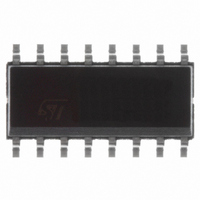
L6910 STMicroelectronics, L6910 Datasheet - Page 20

L6910
Manufacturer Part Number
L6910
Description
IC PWM BUCK BST VM 16SOIC
Manufacturer
STMicroelectronics
Datasheet
1.L6910ATR.pdf
(29 pages)
Specifications of L6910
Pwm Type
Voltage Mode
Number Of Outputs
1
Frequency - Max
230kHz
Duty Cycle
100%
Voltage - Supply
5 V ~ 12 V
Buck
Yes
Boost
Yes
Flyback
No
Inverting
No
Doubler
No
Divider
No
Cuk
No
Isolated
No
Operating Temperature
-40°C ~ 150°C
Package / Case
16-SOIC (3.9mm Width)
Frequency-max
230kHz
Output Voltage
4 V
Mounting Style
SMD/SMT
Lead Free Status / RoHS Status
Contains lead / RoHS non-compliant
Other names
497-3656-5
497-4220-5
497-4220-5
497-4220-5
497-4220-5
Available stocks
Company
Part Number
Manufacturer
Quantity
Price
Part Number:
L6910
Manufacturer:
ST
Quantity:
20 000
Part Number:
L6910A
Manufacturer:
ST
Quantity:
20 000
Company:
Part Number:
L6910ATR
Manufacturer:
INF
Quantity:
2 523
Part Number:
L6910ATR
Manufacturer:
ST
Quantity:
20 000
L6910 - L6910A
9
Double Data Rate (DDR) Memories require a particular Power Management Architecture. This is due to the fact
that the trace between the driving chipset and the memory input must be terminated with resistors.
Since the Chipset driving the Memory has a push pull output buffer, the Termination voltage must be capable
of sourcing and sinking current.
Moreover, the Termination voltage must be equal to one half of the memory supply (the input of the memory is
a differential stage requiring a reference bias midpoint) and in tracking with it. For DDRI the Memory Supply is
2.5V and the Termination voltage is 1.25V while, for DDRII, the Memory Supply is 1.8V and the Termination
voltage is 0.9V. Fig. 23 shows a complete DDRI Memory and Termination Power Supply realized by using 2 x
L6910. The 2.5V section is powering the memory while the 1.25V section is providing the termination voltage.
The tracking between the two sections is realized by providing the EAREF voltage of the 1.25V section through
a resistor divider connected to the 2.5V.
Figure 23. Application idea : DDR Memory Supply
The current required by the memory and the termination supply, depends on the memory type and size.
The figure 24, 25 shows the efficiency of the L6910 for the termination section of the application shown in fig.
23, in sink and source mode. The figures show the efficiency values also when the input voltage is coming di-
rectly from the 12V rail.
20/29
APPLICATION IDEA 1: DDR MEMORY AND TERMINATION SUPPLY
12V
12V
12V
VIN
VIN
VIN
R
R
R
R
R
R
VIN
VIN
VIN
12V
12V
12V
EAREF
EAREF
EAREF
VCC
VCC
VCC
GND
GND
GND
OSC
OSC
OSC
SS
SS
SS
EAREF
EAREF
EAREF
OSC
OSC
OSC
VCC
VCC
VCC
GND
GND
GND
SS
SS
SS
15
15
15
7
7
7
4
4
4
2
2
2
8
8
8
12
12
12
-
-
-
+
+
+
5
5
5
15
15
15
7
7
7
4
4
4
2
2
2
8
8
8
BOOT
BOOT
BOOT
L6910
L6910
L6910
12
12
12
5
5
5
U1
U1
U1
BOOT
BOOT
BOOT
L6910
L6910
L6910
U2
U2
U2
3
3
3
OCSET
OCSET
OCSET
3
3
3
11
11
11
14
14
14
13
13
13
6
6
6
10
10
10
OCSET
OCSET
OCSET
9
9
9
1
1
1
11
11
11
10
10
10
14
14
14
13
13
13
6
6
6
UGATE
UGATE
UGATE
LGATE
LGATE
LGATE
9
9
9
PHASE
PHASE
PHASE
PGND
PGND
PGND
PGOOD
PGOOD
PGOOD
VREF
VREF
VREF
1
1
1
STS11NF3LL
STS11NF3LL
STS11NF3LL
UGATE
UGATE
UGATE
PHASE
PHASE
PHASE
LGATE
LGATE
LGATE
PGND
PGND
PGND
PGOOD
PGOOD
PGOOD
VREF
VREF
VREF
STS8DNF3LL
STS8DNF3LL
STS8DNF3LL
STS11NF3LL
STS11NF3LL
STS11NF3LL
PWRGD
PWRGD
PWRGD
V
V
V
2.5V@15A
2.5V@15A
2.5V@15A
PWRGD
PWRGD
PWRGD
DDQ
DDQ
DDQ
V
V
V
1.25V@ - 5A
1.25V@ - 5A
1.25V@ - 5A
TT
TT
TT
+
+
+
TERMINATION
TERMINATION
TERMINATION
NETWORK
NETWORK
NETWORK
MEMORY
MEMORY
MEMORY
CHIPSET
CHIPSET
CHIPSET
DDR
DDR
DDR
VREF
VREF
VREF


