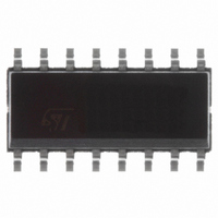
L6910G STMicroelectronics, L6910G Datasheet - Page 20

L6910G
Manufacturer Part Number
L6910G
Description
IC PWM BUCK BST VM 16SOICN
Manufacturer
STMicroelectronics
Datasheet
1.L6910GTR.pdf
(26 pages)
Specifications of L6910G
Pwm Type
Voltage Mode
Number Of Outputs
1
Frequency - Max
230kHz
Duty Cycle
100%
Voltage - Supply
5 V ~ 12 V
Buck
Yes
Boost
Yes
Flyback
No
Inverting
No
Doubler
No
Divider
No
Cuk
No
Isolated
No
Operating Temperature
-40°C ~ 150°C
Package / Case
16-SOIC (3.9mm Width)
Frequency-max
230kHz
Topology
Step Down
Output Voltage
0.9 V to 12 V
Output Current
1300 mA
Switching Frequency
50 KHz to 1000 KHz
Duty Cycle (max)
100 %
Maximum Operating Temperature
+ 150 C
Minimum Operating Temperature
- 40 C
Mounting Style
SMD/SMT
Synchronous Pin
No
Lead Free Status / RoHS Status
Lead free / RoHS Compliant
Available stocks
Company
Part Number
Manufacturer
Quantity
Price
Part Number:
L6910G
Manufacturer:
ST
Quantity:
20 000
Part Number:
L6910GTR
Manufacturer:
ST
Quantity:
20 000
L6910G
9
In some applications the input voltage changes in a very wide range while the output must be regulated to a
fixed value. In this case a Buck-Boost topology can be required in order to keep the output voltage in regulation.
The schematic below shows how to implement a Buck-Boost regulating 5V at the output from both 3.3V and 5V
and 12V input buses.
In a Buck-Boost topology the current is delivered to the output during the OFF phase only. So, for a given current
limit, the maximum output current depends strongly on the duty cycle. Assuming a 100% efficiency and neglect-
ing the current ripple across the inductor, the relationship betweent the current limit and the maximum output
current is the following:
Where I
The worst case is with D
The worst case is with V
Obviously, since the efficiency is lower than 100% and the ripple is usually not negligible, the maximum output
current is always lower than the value calculated in the above formula
Figure 28. Positive buck-boost regulator 3V to 13.2V input / 5V 2.5A Output Circuit
20/26
VIN (3.3V-5V-12V BUSES)
VIN (3.3V-5V-12V BUSES)
VCC (12V BUS)
VCC (12V BUS)
GNDCC
GNDCC
GNDCC
GNDIN
GNDIN
GNDIN
APPLICATION IDEA 2: POSITIVE BUCK-BOOST REGULATOR 3V TO 13.2V
INPUT / 5V 2.5A OUTPUT
LIM
is the current limit and D is the duty cycle of the application.
C8
C8
C6
C6
G1
G1
INMIN
MAX
R7
R7
. Since, in a Buck-Boost application, D is given by the following formula:
C7
C7
C7
.
C5
C5
EAREF
EAREF
D1
D1
GND
GND
VCC
VCC
OSC
OSC
SS
SS
15
15
7
7
4
4
2
2
8
8
12
12
5
5
L6910/A
L6910/A
C9
C9
BOOT
BOOT
U1
U1
C10
C10
I
R1
R1
OMAX
3
3
R5
R5
R6
R6
D
OCSET
OCSET
6
6
=
C3
C3
11
11
10
10
14
14
13
13
=
9
9
1
1
---------------------- -
V
I
LIM
C4
C4
VREF
VREF
PGND
PGND
IN
UGATE
UGATE
PHASE
PHASE
LGATE
LGATE
PGOOD
PGOOD
V
+
O
⋅
V
(
1 D
O
–
C12
C12
Q1
Q1
Q2
Q2
Q2
)
R4
R4
R3
R3
D2
D2
C11
C11
L1
L1
Q3
Q3
C1- C2
C1- C2
Q4
Q4
C13
C13-14
C13
-14
-14
R2
R2
VOUT ( 5V 2.5A )
VOUT ( 5V 2.5A )
GNDOUT
GNDOUT


