LT3574IMS#PBF Linear Technology, LT3574IMS#PBF Datasheet - Page 16

LT3574IMS#PBF
Manufacturer Part Number
LT3574IMS#PBF
Description
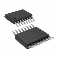
IC PWM FLYBCK ISO CM 16MSOP
Manufacturer
Linear Technology
Type
Flyback, Isolated, PWM - Current Moder
Datasheet
1.LT3574EMSPBF.pdf
(24 pages)
Specifications of LT3574IMS#PBF
Internal Switch(s)
Yes
Synchronous Rectifier
No
Number Of Outputs
1
Voltage - Output
Adj to 60V
Current - Output
650mA
Frequency - Switching
40kHz ~ 1MHz
Voltage - Input
3 ~ 40 V
Operating Temperature
-40°C ~ 125°C
Mounting Type
*
Package / Case
16-MSOP
Voltage - Supply
3 V ~ 40 V
Frequency-max
1MHz
Duty Cycle
52%
Pwm Type
Current Mode
Buck
No
Boost
No
Flyback
Yes
Inverting
No
Doubler
No
Divider
No
Cuk
No
Isolated
Yes
Lead Free Status / RoHS Status
Lead free / RoHS Compliant
Available stocks
Company
Part Number
Manufacturer
Quantity
Price
LT3574
BIAS winding turns ratio is selected to program the BIAS
voltage to 3~5V. The BIAS voltage shall not exceed the
input voltage.
The turns ratio is then selected as primary: secondary:
BIAS = 3:1:1.
2. Select the transformer primary inductance for target
The LT3574 requires a minimum amount of time to sample
the output voltage during the off-time. This off-time,
t
conditions. The converter also has a minimum current limit,
I
the minimum required inductance as defined as:
The transformer primary inductance also affects the
switching frequency which is related to the output ripple. If
above the minimum inductance, the transformer’s primary
inductance may be selected for a target switching frequency
range in order to minimize the output ripple.
The following equation estimates the switching frequency.
Table 7. Switching Frequency at Different Primary Inductance
at I
Note: The switching frequency is calculated at maximum output.
applications inForMation
OFF(MIN)
MIN
PK
switching frequency.
L
f
SW
, of 175mA to help create this off-time. This defines
MIN
L (µH)
=
120
30
60
, shall be greater than 350ns over all operating
=
t
N V
ON
(
+
OUT
1
I
MIN
t
OFF
+
V
=
f
F
SW
)
V
•
I
AT V
IN
(kHz)
PK
317
159
t
79
OFF MIN
L
IN(MIN)
+
(
N
PS
)
(
1
V
OUT
f
I
SW
PK
AT V
+
(kHz)
373
187
93
V
IN(MAX)
F
)
L
In this design example, the minimum primary inductance is
used to achieve a nominal switching frequency of 350kHz
at full load. The PA2627NL from Pulse Engineering is
chosen as the flyback transformer.
Given the turns ratio and primary inductance, a custom-
ized transformer can be designed by magnetic component
manufacturer or a multi-winding transformer such as a
Coiltronics Versa-Pac may be used.
3. Select the output diodes and output capacitor.
The output diode voltage stress V
the output voltage and reflection of input voltage to the
secondary side. The average diode current is the load
current.
The output capacitor should be chosen to minimize the
output voltage ripple while considering the increase in
size and cost of a larger capacitor. The following equation
calculates the output voltage ripple.
4. Select the snubber circuit to clamp the switch voltage
A flyback converter generates a voltage spike during switch
turn-off due to the leakage inductance of the transformer.
In order to clamp the voltage spike below the maximum
rating of the switch, a snubber circuit is used. There are
many types of snubber circuits, for example R-C, R-C-D and
Zener clamps. Among them, RCD is widely used. Figure 9
shows the RCD snubber in a flyback converter.
A typical switch node waveform is shown in Figure 10.
spike.
V
DV
D
MAX
=
V
OUT
=
2
LI
+
CV
V
2
N
OUT
IN
PK
D
is the summation of
3574f


