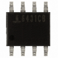
ISL6431CB Intersil, ISL6431CB Datasheet - Page 8

ISL6431CB
Manufacturer Part Number
ISL6431CB
Description
IC CNTRLR PWM SYNC BUCK 8-SOIC
Manufacturer
Intersil
Datasheet
1.ISL6431CB.pdf
(10 pages)
Specifications of ISL6431CB
Pwm Type
Voltage Mode
Number Of Outputs
1
Frequency - Max
340kHz
Duty Cycle
100%
Voltage - Supply
4.5 V ~ 5.5 V
Buck
Yes
Boost
No
Flyback
No
Inverting
No
Doubler
No
Divider
No
Cuk
No
Isolated
No
Operating Temperature
0°C ~ 70°C
Package / Case
8-SOIC (3.9mm Width)
Frequency-max
340kHz
Lead Free Status / RoHS Status
Contains lead / RoHS non-compliant
The response time to a transient is different for the
application of load and the removal of load. The following
equations give the approximate response time interval for
application and removal of a transient load:
where: I
response time to the application of load, and t
response time to the removal of load. The worst case
response time can be either at the application or removal of
load. Be sure to check both of these equations at the
minimum and maximum output levels for the worst case
response time.
Input Capacitor Selection
Use a mix of input bypass capacitors to control the voltage
overshoot across the MOSFETs. Use small ceramic
capacitors for high frequency decoupling and bulk capacitors
to supply the current needed each time Q
small ceramic capacitors physically close to the MOSFETs
and between the drain of Q
The important parameters for the bulk input capacitor are the
voltage rating and the RMS current rating. For reliable
operation, select the bulk capacitor with voltage and current
ratings above the maximum input voltage and largest RMS
current required by the circuit. The capacitor voltage rating
should be at least 1.25 times greater than the maximum
input voltage and a voltage rating of 1.5 times is a
conservative guideline. The RMS current rating requirement
for the input capacitor of a buck regulator is approximately
1/2 the DC load current.
For a through hole design, several electrolytic capacitors may
be needed. For surface mount designs, solid tantalum
capacitors can be used, but caution must be exercised with
regard to the capacitor surge current rating. These capacitors
must be capable of handling the surge-current at power-up.
Some capacitor series available from reputable manufacturers
are surge current tested.
MOSFET Selection/Considerations
The ISL6431 requires two N-Channel power MOSFETs for use
in a synchronous buck configuration. These should be selected
based upon r
management requirements.
In high-current applications, the MOSFET power
dissipation, package selection and heatsink are the
dominant design factors. The power dissipation includes
two loss components; conduction loss and switching loss.
The conduction losses are the largest component of power
dissipation for both the upper and the lower MOSFETs.
These losses are distributed between the two MOSFETs
according to duty factor (see the equations below). Only
the upper MOSFET has switching losses, since the lower
MOSFETs body diode or an external Schottky rectifier
t
RISE
=
TRAN
V
L x I
IN
DS(ON)
- V
is the transient load current step, t
TRAN
OUT
, gate supply requirements, and thermal
1
and the source of Q
t
FALL
8
=
L x I
V
1
OUT
turns on. Place the
TRAN
FALL
2
RISE
.
is the
is the
ISL6431
across the lower MOSFET clamps the switching node
before the synchronous rectifier turns on. These equations
assume linear voltage-current transitions and do not
adequately model power loss due the reverse-recovery of
the lower MOSFET’s body diode. The gate-charge losses
are dissipated by the ISL6431 and don't heat the
MOSFETs. However, large gate-charge increases the
switching interval, t
switching losses. Ensure that both MOSFETs are within
their maximum junction temperature at high ambient
temperature by calculating the temperature rise according
to package thermal-resistance specifications. A separate
heatsink may be necessary depending upon MOSFET
power, package type, ambient temperature and air flow.
Given the reduced available gate bias voltage (5V), logic-
level or sub-logic-level transistors have to be used for both
N-MOSFETs. Caution should be exercised with devices
exhibiting very low V
threshold could be conducive to some shoot-through (due to
the Miller effect), in spite of the counteracting circuitry
present aboard the ISL6431.
Figure 7 shows the upper gate drive (BOOT pin) supplied by a
bootstrap circuit from V
develops a floating supply voltage referenced to the PHASE
pin. The supply is refreshed to a voltage of V
diode drop (V
P
Where: D is the duty cycle = V
P
UPPER
LOWER
+
-
ISL6431
+5V
VCC
FIGURE 7. UPPER GATE DRIVE BOOTSTRAP
t
F
= Io
= Io
SW
S
is the switching frequency.
2
2
is the switch ON time, and
D
x r
x r
) each time the lower MOSFET, Q
DS(ON)
DS(ON)
+ V
GND
D
BOOT
SW
BOOT
UGATE
PHASE
LGATE
D
GS(ON)
-
CC
x D +
which increases the upper MOSFET
x (1 - D)
. The boot capacitor, C
C
characteristics, as the low gate
1
2
BOOT
OUT
Io x V
Q1
Q2
+5V
/ V
IN
IN
x t
,
SW
CC
x F
NOTE:
V
NOTE:
V
G-S
G-S
less the boot
S
BOOT
2
, turns on.
V
V
CC
CC
,
-V
D


