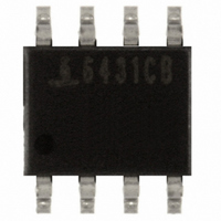
ISL6431CB Intersil, ISL6431CB Datasheet - Page 4

ISL6431CB
Manufacturer Part Number
ISL6431CB
Description
IC CNTRLR PWM SYNC BUCK 8-SOIC
Manufacturer
Intersil
Datasheet
1.ISL6431CB.pdf
(10 pages)
Specifications of ISL6431CB
Pwm Type
Voltage Mode
Number Of Outputs
1
Frequency - Max
340kHz
Duty Cycle
100%
Voltage - Supply
4.5 V ~ 5.5 V
Buck
Yes
Boost
No
Flyback
No
Inverting
No
Doubler
No
Divider
No
Cuk
No
Isolated
No
Operating Temperature
0°C ~ 70°C
Package / Case
8-SOIC (3.9mm Width)
Frequency-max
340kHz
Lead Free Status / RoHS Status
Contains lead / RoHS non-compliant
Electrical Specifications
Functional Pin Descriptions
VCC (Pin 5)
This is the main bias supply for the ISL6431, as well as the
lower MOSFET’s gate. Connect a well-decoupled 5V supply
to this pin.
FB (Pin 6)
This pin is the inverting input of the internal error amplifier.
Use this pin, in combination with the COMP/OCSET pin, to
compensate the voltage-control feedback loop of the
converter.
GND (Pin 3)
This pin represents the signal and power ground for the IC.
Tie this pin to the ground island/plane through the lowest
impedance connection available.
PHASE (Pin 8)
Connect this pin to the upper MOSFET source. This pin is
used to monitor the voltage drop across the upper MOSFET
for overcurrent protection. This pin is also monitored by the
continuously adaptive shoot-through protection circuitry to
determine when the upper MOSFET has turned off.
UGATE (Pin 2)
Connect this pin to the upper MOSFET’s gate. This pin
provides the PWM-controlled gate drive for the upper
MOSFET. This pin is also monitored by the adaptive shoot-
through protection circuitry to determine when the upper
MOSFET has turned off. Do not insert any circuitry between
this pin and the gate of the upper MOSFET, as it may
interfere with the internal adaptive shoot-through protection
circuitry and render it ineffective.
BOOT (Pin 1)
This pin provides ground referenced bias voltage to the
upper MOSFET driver. A bootstrap circuit is used to create a
voltage suitable to drive a logic-level N-channel MOSFET.
COMP/OCSET (Pin 7)
This is a multiplexed pin. During a short period of time
following power-on reset (POR), this pin is used to determine
the overcurrent threshold of the converter. Connect a
resistor (R
MOSFET (V
Lower Gate Sink Current
PROTECTION / DISABLE
OCSET Current Source
Disable Threshold
PARAMETER
OCSET
CC
). R
) from this pin to the drain of the upper
OCSET
, an internal 20 A current source
4
I
LGATE-SNK
Recommended Operating Conditions, Unless Otherwise Noted V
V
SYMBOL
I
DISABLE
OCSET
ISL6431CB
ISL6431IB
ISL6431CB
ISL6431IB
ISL6431CB
ISL6431IB
TEST CONDITIONS
ISL6431
(I
set the converter overcurrent (OC) trip point according to the
following equation:
Internal circuitry of the ISL6431 will not recognize a voltage
drop across R
across R
overcurrent trip point to:
An overcurrent trip cycles the soft-start function.
Pulling OCSET to a level below 0.8V will disable the
controller. Disabling the ISL6431 causes the oscillator to
stop, the LGATE and UGATE outputs to be held low, and the
softstart circuitry to re-arm.
During soft-start, and all the time during normal converter
operation, this pin represents the output of the error
amplifier. Use this pin, in combination with the FB pin, to
compensate the voltage-control feedback loop of the
converter.
LGATE (Pin 4)
Connect this pin to the lower MOSFET’s gate. This pin
provides the PWM-controlled gate drive for the lower
MOSFET. This pin is also monitored by the adaptive shoot-
through protection circuitry to determine when the lower
MOSFET has turned off. Do not insert any circuitry between
this pin and the gate of the lower MOSFET, as it may
interfere with the internal adaptive shoot-through protection
circuitry and render it ineffective.
Functional Descriptions
Initialization
The ISL6431 automatically initializes upon receipt of power.
The Power-On Reset (POR) function continually monitors the
bias voltage at the VCC pin. The POR function initiates the
Overcurrent Protection (OCP) sampling and hold operation
after the supply voltage exceeds its POR threshold. Upon
I
I
PEAK
PEAK
OCSET
=
=
), and the upper MOSFET on-resistance (r
OCSET
I
-------------------------------------------------
--------------------- -
r
OCSET
DS ON
0.5V
r
OCSET
DS ON
xR
that is greater than 0.5V will set the
OC SET
CC
larger than 0.5V. Any voltage drop
MIN
17
14
= 5.0V 5% and T
-
-
-
-
TYP
2.0
2.0
20
20
-
-
A
= 25
MAX
0.8
0.8
22
24
-
-
o
C (Continued)
DS(ON)
UNITS
A
A
V
V
A
A
)


