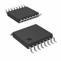
LM5026MT/NOPB National Semiconductor, LM5026MT/NOPB Datasheet - Page 14

LM5026MT/NOPB
Manufacturer Part Number
LM5026MT/NOPB
Description
CURRENT MODE-ACTIVE RESET
Manufacturer
National Semiconductor
Series
PowerWise®r
Datasheet
1.LM5026MTNOPB.pdf
(22 pages)
Specifications of LM5026MT/NOPB
Pwm Type
Current Mode
Number Of Outputs
2
Frequency - Max
1MHz
Duty Cycle
92.5%
Voltage - Supply
13 V ~ 100 V
Buck
Yes
Boost
Yes
Flyback
Yes
Inverting
Yes
Doubler
No
Divider
No
Cuk
No
Isolated
Yes
Operating Temperature
-40°C ~ 125°C
Package / Case
16-TSSOP
Frequency-max
1MHz
For Use With
LM5026EVAL - BOARD EVALUATION LM5026
Lead Free Status / RoHS Status
Lead free / RoHS Compliant
Other names
*LM5026MT
*LM5026MT/NOPB
LM5026MT
*LM5026MT/NOPB
LM5026MT
Available stocks
Company
Part Number
Manufacturer
Quantity
Price
Company:
Part Number:
LM5026MT/NOPB
Manufacturer:
TI
Quantity:
3 000
www.national.com
Oscillator and Sync Capability
The LM5026 oscillator frequency is set by the external resis-
tance connected between the RT pin and ground (AGND). To
set a desired oscillator frequency (F) the necessary value of
total R
The R
and connected directly to the pins of the IC (RT and AGND).
The SYNC pin can be used to synchronize the internal oscil-
lator to an external clock. An open drain output is the recom-
mended interface between the external clock to the LM5026
SYNC pin as illustrated in
must be greater than 15 ns. The external clock frequency
must be a higher than the free running frequency set by the
R
T
resistance.
pin is used as an input, the driving source should be
current limited to less than 5 mA. For example, the
T
T
resistor(s) should be located very close to the device
resistance can be calculated from:
FIGURE 8. Sync from External Clock
Figure
8. The clock pulse width
FIGURE 7. Hiccup Over-Load Restart Timing
20147919
14
Multiple LM5026 devices can be synchronized together sim-
ply by connecting the devices SYNC pins together as shown
in
tential differences between devices are minimized. In this
configuration all of the devices will be synchronized to the
highest frequency device. The internal block diagram of the
oscillator and synchronization circuit is shown in
The SYNC I/O pin is a CMOS buffer with pull-up current lim-
ited to 200 µA. If an external device forces the SYNC pin low
before the internal oscillator ramp completes its charging cy-
cle, the ramp will be reset and another cycle begins. If the
SYNC pins of multiple LM5026 devices are connected to-
gether, the first SYNC pin that pulls low will reset the oscillator
RAMP of all other devices. All controllers will operate in phase
when synchronized using the SYNC I/O feature. Up to five
LM5026 devices can be synchronized using this technique.
Figure
external trigger for a delayed restart sequence could
come an over-temperature protection circuit.
FIGURE 9. Sync from Multiple Devices
9. Care should be taken to ensure the ground po-
20147920
20147918
Figure
10.


