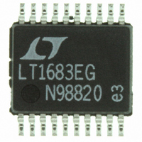
LTC1922EG-1#PBF Linear Technology, LTC1922EG-1#PBF Datasheet - Page 13

LTC1922EG-1#PBF
Manufacturer Part Number
LTC1922EG-1#PBF
Description
IC CTLR PWM SYNC 20SSOP
Manufacturer
Linear Technology
Datasheet
1.LTC1922EG-1PBF.pdf
(24 pages)
Specifications of LTC1922EG-1#PBF
Pwm Type
Voltage/Current Mode
Number Of Outputs
1
Frequency - Max
1MHz
Duty Cycle
99%
Buck
No
Boost
No
Flyback
No
Inverting
No
Doubler
No
Divider
No
Cuk
No
Isolated
Yes
Operating Temperature
-40°C ~ 85°C
Package / Case
20-SSOP
Frequency-max
1MHz
Lead Free Status / RoHS Status
Lead free / RoHS Compliant
Voltage - Supply
-
Available stocks
Company
Part Number
Manufacturer
Quantity
Price
OPERATIO
Off-Line Bias Supply Generation
If a regulated bias supply is not available to provide V
voltage to the LTC1922-1 and supporting circuitry, one
must be generated. Since the power requirement is small,
approximately 1W, and the regulation is not critical, a
simple open-loop method is usually the easiest and lowest
cost approach. One method that works well is to add a
winding to the main power transformer, and post regulate
the resultant square wave with an L-C filter (see Figure 5a).
The advantage of this approach is that it maintains decent
regulation as the supply voltage varies, and it does not
require full safety isolation from the input winding of the
transformer. Some manufacturers include a primary wind-
ing for this purpose in their standard product offerings as
well. A different approach is to add a winding to the output
inductor and peak detect and filter the square wave signal
(see Figure 5b). The polarity of this winding is designed so
that the positive voltage square wave is produced while the
output inductor is freewheeling. An advantage of this
technique over the previous is that it does not require a
separate filter inductor and since the voltage is derived
from the well-regulated output voltage, it is also well
controlled. One disadvantage is that this winding will
require the same safety isolation that is required for the
main transformer. Another disadvantage is that a much
larger V
CC
Figure 5a. Auxiliary Winding Bias Supply
V
V
filter capacitor is needed, since it does not
IN
CC
Figure 5b. Output Inductor Bias Supply
R
START
U
0.1 F
15V*
*OPTIONAL
ISO BARRIER
R
START
C
HOLD
+
V
IN
L
OUT
C
HOLD
2k
1922 F05a
+
V
CC
1922 F05b
V
0.1 F
OUT
CC
generate a voltage as the output is first starting up, or
during short-circuit conditions.
Programming the LTC1922-1 Oscillator
The high accuracy LTC1922-1 oscillator circuit provides
flexibility to program the switching frequency, slope com-
pensation, and synchronization with minimal external
components. The LTC1922-1 oscillator circuitry produces
a 3.8V peak-to-peak amplitude ramp waveform on C
a narrow pulse on SYNC that can be used to synchronize
other PWM chips. Typical maximum duty cycles of 99%
are obtained at 300kHz and 97% at 1MHz. The large
amplitude ramp provides a high degree of noise margin. A
compensating slope current is derived from the oscillator
ramp waveform and sourced out of CS.
The desired amount of slope compensation is selected
with single external resistor (or no resistor), if not re-
quired. A capacitor to GND on C
frequency. The C
to a high value (>10mA). The dedicated SYNC I/O pin easily
achieves synchronization. The LTC1922-1 can be set up to
either synchronize other PWM chips or be synchronized
by another chip or external clock source. The 1.8V SYNC
threshold allows the LTC1922-1 to be synchronized di-
rectly from all standard 3V and 5V logic families.
Design Procedure:
1. Choose C
switching frequency selected must be consistent with the
power magnetics and output power level. This is detailed
in the Transformer Design section. In general, increasing
the switching frequency will decrease the maximum achiev-
able output power, due to limitations of maximum duty
cycle imposed by transformer core reset and ZVS. Re-
member that the output frequency is 1/2 that of the
oscillator.
Example: Desired f
C
C
value of 150pF. A 5% or better tolerance multilayer NPO
or X7R ceramic capacitor is recommended for best
performance.
T
T
= 1/(20k • 330kHz) = 152pF, choose closest standard
= 1/(20k • f
T
for the desired oscillator frequency. The
T
OSC
ramp discharge current is internally set
OSC
)
= 330kHz
T
programs the switching
LTC1922-1
13
T
and


