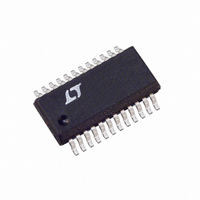
LTC3722EGN-1#PBF Linear Technology, LTC3722EGN-1#PBF Datasheet - Page 22

LTC3722EGN-1#PBF
Manufacturer Part Number
LTC3722EGN-1#PBF
Description
IC CTLR PWM CURRENT-MODE 24SSOP
Manufacturer
Linear Technology
Datasheet
1.LTC3722EGN-1PBF.pdf
(28 pages)
Specifications of LTC3722EGN-1#PBF
Pwm Type
Current Mode, Full Bridge
Number Of Outputs
1
Frequency - Max
1MHz
Duty Cycle
98.5%
Voltage - Supply
3.8 V ~ 10.3 V
Buck
No
Boost
No
Flyback
No
Inverting
No
Doubler
No
Divider
Yes
Cuk
No
Isolated
Yes
Operating Temperature
-40°C ~ 85°C
Package / Case
24-SSOP
Frequency-max
1MHz
Lead Free Status / RoHS Status
Lead free / RoHS Compliant
Available stocks
Company
Part Number
Manufacturer
Quantity
Price
LTC3722-1/LTC3722-2
operaTion
Power Transformer
Switching frequency, core material characteristics, series
resistance and input/output voltages all play an important
role in transformer selection. Close attention also needs
to be paid to leakage and magnetizing inductances as
they play an important role in how well the converter will
achieve ZVS. Planar magnetics are very well suited to
these applications because of their excellent control of
these parameters.
Turns Ratio
The required turns ratio for a current doubler secondary
is given below. Depending on the magnetics selected, this
value may need to be reduced slightly.
Turns ratio formula:
where:
Output Capacitors
Output capacitor selection has a dramatic impact on ripple
voltage, dynamic response to transients and stability.
Capacitor ESR along with output inductor ripple current
will determine the peak-to-peak voltage ripple on the out-
put. The current doubler configuration is advantageous
because it has inherent ripple current reduction. The dual
output inductors deliver current to the output capacitor 180
degrees out-of-phase, in effect, partially canceling each
other’s ripple current. This reduction is maximized at high
duty cycle and decreases as the duty cycle reduces. This
means that a current doubler converter requires less output
capacitance for the same performance as a conventional
converter. By determining the minimum duty cycle for the
converter, worse-case V
following formula:
V
ORIPPLE
V
D
N
IN(MIN)
MAX
=
V
IN MIN
= Maximum duty cycle of controller (DC
(
=
• 2
= Minimum V
I
RIPPLE
V
)
OUT
•
D
MAX
•
ESR
OUT
IN
=
for operation
ripple can be derived by the
L
O
V
O
• •
2
•
ESR
f
SW
( – )( –
1
D
MAX
1 2 2 D)
)
where:
D = minimum duty cycle
f
L
ESR = output capacitor series resistance
The amount of bulk capacitance required is usually system
dependent, but has some relationship to output inductance
value, switching frequency, load power and dynamic load
characteristics. Polymer electrolytic capacitors are the
preferred choice for their combination of low ESR, small
size and high reliability. For less demanding applications,
or those not constrained by size, aluminum electrolytic
capacitors are commonly applied. Most DC/DC convert-
ers in the 100kHz to 300kHz range use 20µF to 25µF of
bulk capacitance per watt of output power. Converters
switching at higher frequencies can usually use less bulk
capacitance. In systems where dynamic response is critical,
additional high frequency capacitors, such as ceramics,
can substantially reduce voltage transients.
Power MOSFETs
The full bridge power MOSFETs should be selected for
their R
rated MOSFET available for a given input voltage range
leaving at least a 20% voltage margin. Conduction losses
are directly proportional to R
has two MOSFETs in the power path most of the time,
conduction losses are approximately equal to:
Switching losses in the MOSFETs are dominated by the
power required to charge their gates, and turn-on and
turn-off losses. At higher power levels, gate charge power
is seldom a significant contributor to efficiency loss. ZVS
operation virtually eliminates turn-on losses. Turn-off
losses are reduced by the use of an external drain to source
snubber capacitor and/or a very low resistance turn-off
driver. If synchronous rectifier MOSFETs are used on the
secondary, the same general guidelines apply. Keep in
mind, however, that the BV
be greater than V
SW
O
2
= output inductance
= oscillator frequency
•
R
DS(ON)
DS ON
(
and BV
)
• ,
I
2
IN(MAX)
where
DSS
ratings. Select the lowest BV
/N, depending on how well the
DSS
I
DS(ON)
=
rating needed for these can
2
I
O
N
. Since the full bridge
372212fa
DSS


