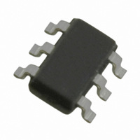
LT6656ACS6-4.096#TRPBF Linear Technology, LT6656ACS6-4.096#TRPBF Datasheet - Page 9

LT6656ACS6-4.096#TRPBF
Manufacturer Part Number
LT6656ACS6-4.096#TRPBF
Description
IC VREF PREC 5MA 4.096V TSOT23-6
Manufacturer
Linear Technology
Datasheet
1.LT6656BCS6-2.5TRMPBF.pdf
(18 pages)
Specifications of LT6656ACS6-4.096#TRPBF
Reference Type
Series
Voltage - Output
4.096V
Tolerance
±0.05%
Temperature Coefficient
10ppm/°C
Voltage - Input
4.596 ~ 18 V
Number Of Channels
1
Current - Quiescent
850nA
Current - Output
5mA
Operating Temperature
0°C ~ 70°C
Mounting Type
Surface Mount
Package / Case
SOT-23-6 Thin, TSOT-23-6
Lead Free Status / RoHS Status
Lead free / RoHS Compliant
Current - Cathode
-
Available stocks
Company
Part Number
Manufacturer
Quantity
Price
Part Number:
LT6656ACS6-4.096#TRPBFLT6656ACS6-4.096#PBF/AI/BC/BI
Manufacturer:
LT
Quantity:
32
applicaTions inForMaTion
Long Battery Life
Series references have a large advantage over shunt style
references. Shunt references require a resistor from the
power supply to operate. This resistor must be chosen
to supply the maximum current that can be demanded by
the load. When the load is not operating at this maximum
current, the shunt reference must always sink this current,
resulting in high dissipation and shortened battery life.
The LT6656 series reference does not require a current
setting resistor and is specified to operate with any supply
from 1.5V to 18V, depending on the output voltage option,
load current and operating temperature (see Dropout
Voltage and Minimum Input Voltage in the Typical Perfor-
mance Characteristics). When the load does not demand
current, the LT6656 reduces its dissipation and battery life
is extended. If the reference is not delivering load current,
it dissipates only a few µW, yet the same connection can
deliver 5mA of load current when required.
Start-Up
To ensure proper start-up, the output voltage should be
between –0.3V and the rated output voltage. If the output
load may be driven more than 0.3V below ground, a low
forward voltage schottky diode from the output to ground
is required. The turn-on characteristics can be seen in
Figure 1.
1V/DIV
Figure 1. LT6656-2.5 Turn-On Characteristics, C
V
OUT
V
IN
1ms/DIV
6656 F01
L
= 1µF
Output Voltage Options
The performance of the LT6656 is consistent for the 2.048V
to 5V options. The 1.25V option has slightly reduced load
regulation, and unlike the higher voltage options, the
minimum operating supply voltage is limited by internal
circuitry rather than the output voltage.
Parameters that are based on changes in the output voltage,
such as load regulation and hysteresis, remain proportional
to the output voltage and are specified in relative units,
for example, parts per million (ppm). Parameters that
are not based on changes in the output voltage, such as
supply current and reverse input current, are the same
for all options.
The bandwidth of the LT6656 decreases with higher output
voltage. This causes parameters that are affected by both
bandwidth and output voltage, such as wideband noise
and output impedance, to increase less with higher output
voltage.
Bypass and Load Capacitance
The LT6656 voltage reference needs a 0.1μF input bypass
capacitor placed within an inch of the input pin. An ad-
ditional 2.2μF capacitor should be used when the source
impedance of the input supply is high or when driving
heavy loads. The bypassing of other local devices may
serve as the required components. The output of the
LT6656 requires a capacitance of 1µF or larger. The LT6656
is stable with a wide variety of capacitor types including
ceramic, tantalum and electrolytic due to its low sensitivity
to ESR (5Ω or less).
The test circuit in Figure 2 was used to test the response
and stability of the LT6656 to various load currents. The
resultant transient responses can be seen in Figure 3 and
Figure 4. The large scale output response to a 500mV input
step is shown in Figure 5 with a more detailed photo and
description in the Output Settling section.
V
3V
0.1µF
IN
C
IN
Figure 2. Transient Load Test Circuit
LT6656-2.5
C
1µF
L
R1
R2
2N7000
LT6656
V
GEN
6656 F02
6656fa
3V


