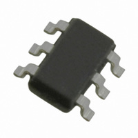
LT6656ACS6-4.096#TRPBF Linear Technology, LT6656ACS6-4.096#TRPBF Datasheet - Page 10

LT6656ACS6-4.096#TRPBF
Manufacturer Part Number
LT6656ACS6-4.096#TRPBF
Description
IC VREF PREC 5MA 4.096V TSOT23-6
Manufacturer
Linear Technology
Datasheet
1.LT6656BCS6-2.5TRMPBF.pdf
(18 pages)
Specifications of LT6656ACS6-4.096#TRPBF
Reference Type
Series
Voltage - Output
4.096V
Tolerance
±0.05%
Temperature Coefficient
10ppm/°C
Voltage - Input
4.596 ~ 18 V
Number Of Channels
1
Current - Quiescent
850nA
Current - Output
5mA
Operating Temperature
0°C ~ 70°C
Mounting Type
Surface Mount
Package / Case
SOT-23-6 Thin, TSOT-23-6
Lead Free Status / RoHS Status
Lead free / RoHS Compliant
Current - Cathode
-
Available stocks
Company
Part Number
Manufacturer
Quantity
Price
Part Number:
LT6656ACS6-4.096#TRPBFLT6656ACS6-4.096#PBF/AI/BC/BI
Manufacturer:
LT
Quantity:
32
LT6656
applicaTions inForMaTion
Output Settling
The output of the LT6656 is primarily designed to source
current into a load, but is capable of sinking current to
aid in output transient recovery. The output stage uses a
class B architecture to minimize quiescent current and
has a crossover dead band as the output transitions from
sourcing to sinking current.
0
Figure 5. Output Response to 0.5V
V
V
I
I
V
OUT
OUT
OUT
OUT
OUT
V
IN
Figure 3. Transient Response, 0µA to 100µA Load Step
(R2 = 24.9k, R1 = Open)
Figure 4. Transient Response, 1mA to 2mA Load Step
(R1 = R2 = 2.49k)
100µA
2.52V
2.50V
2.48V
2.52V
2.50V
2.48V
3.25V
2.75V
1mA
2mA
2.7V
2.5V
2.3V
0µA
5ms/DIV
5ms/DIV
5ms/DIV
P-P
Step on V
IN
, C
6656 F03
6656 F04
6656 F05
L
= 1µF , I
L
= 0
The settling time is typically less than 8ms for output loads
up to 5mA, however the time required to settle when the
load is turned off or in response to an input transient can be
significantly longer due to the dead band (shown in Figure
7). During this interval the output stage is neither sourcing
nor sinking current so the settling time is dominated by
the ability of the application circuit to discharge the output
capacitor to the voltage at which the sourcing circuitry
in the output stage reactivates. Larger load currents will
decrease the settling time and higher output capacitance
will increase the settling time.
In application circuits where the LT6656 is experiencing
a load step greater than 5µA, such as an ADC reference
and supply implementation, the settling time will typically
remain less than 8ms, regardless of the output settling
from a previous load step.
The settling time can be estimated by the following
equation:
The deadband is ≈7mV for the 2.5V option, is proportional
to the voltage option (i.e., ≈14mV for the 5V option) and
can double due to variations in processing.
The graph in Figure 6 shows the settling time versus load
step with no load and with a constant 2µA load applied.
Note the settling time can be longer with load steps that
are not large enough to activate the sinking side of the
output stage.
Settling time
Figure 6. Output Settling Time to 0.05% vs Load Step
30
25
20
15
10
0.001
5
0
2.5V OPTION
V
C
IN
L
= 1µF
≈
= 3V
2
0.01
(
Deadband C
LOAD STEP (mA)
I
L
∆I
STEP TO ZERO
0.1
∆I
STEP TO 2µA
L
= LOAD
L
= LOAD
)( )
∆I
LOAD STEP
L
L
= ZERO TO
1
+
(
V
6656 F06
OUT
10
)( .
0 8
m
s s V / )
6656fa


