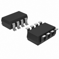
AD7740YRT-REEL7 Analog Devices Inc, AD7740YRT-REEL7 Datasheet - Page 5

AD7740YRT-REEL7
Manufacturer Part Number
AD7740YRT-REEL7
Description
IC CONVERTER V TO FREQ SOT-23-8
Manufacturer
Analog Devices Inc
Type
Voltage to Frequencyr
Datasheet
1.AD7740YRMZ.pdf
(11 pages)
Specifications of AD7740YRT-REEL7
Rohs Status
RoHS non-compliant
Frequency - Max
500kHz
Full Scale
±50ppm/°C
Linearity
±0.012%
Mounting Type
Surface Mount
Package / Case
SOT-23-8
Converter Function
VFC
Full Scale Frequency
1000
Power Supply Requirement
Single
Single Supply Voltage (max)
5.25V
Single Supply Voltage (min)
3V
Dual Supply Voltage (typ)
Not RequiredV
Dual Supply Voltage (min)
Not RequiredV
Dual Supply Voltage (max)
Not RequiredV
Operating Temperature (min)
-40C
Operating Temperature (max)
105C
Operating Temperature Classification
Industrial
Package Type
SOT-23
Lead Free Status / Rohs Status
Not Compliant
TERMINOLOGY
INTEGRAL NONLINEARITY
For the VFC, Integral Nonlinearity (INL) is a measure of the maxi-
mum deviation from a straight line passing through the actual
endpoints of the VFC transfer function. The error is expressed in
% of the actual frequency span:
OFFSET ERROR
Ideally, the output frequency for 0 V input voltage is 10% of
f
to the input is the offset error at BUF = 0. In buffered mode the
minimum output frequency (corresponding to 0.10 V minimum
input voltage) is 13.2% of f
from this value referred to the input is the offset error at BUF = 1.
Offset error is expressed in mV.
GAIN ERROR
This is a measure of the span error of the VFC. The gain is the
scale factor that relates the input VIN to the output FOUT.
The gain error is the deviation in slope of the actual VFC transfer
characteristic from the ideal expressed as a percentage of the full-
scale span. See Figure 2.
OFFSET ERROR DRIFT
This is a measure of the change in Offset Error with changes in
temperature. It is expressed in µV/°C.
GAIN ERROR DRIFT
This is a measure of the change in Gain Error with changes in
temperature. It is expressed in (ppm of span)/°C.
CLKIN
in unbuffered mode. The deviation from this value referred
Frequency Span = FOUT(max) – FOUT(min)
CLKIN
at V
REF
= 2.5 V. The deviation
POWER SUPPLY REJECTION RATIO (PSRR)
This indicates how the apparent input voltage of the VFC is
affected by changes in the supply voltage. The input voltage is
kept constant at 2 V, V
in input voltage to the change in VDD is measured in dBs.
10% at 3.3 V and ±5% at 5 V. The ratio of the apparent change
FREQUENCY
f
CLKIN
0.9 f
0.1
OUTPUT
FOUT
CLKIN
0
OFFSET
ERROR
REF
is 2.5 V and the VDD supply is varied
REFIN
GAIN ERROR
AD7740
IDEAL
WITH OFFSET
ERROR ONLY
WITH OFFSET
ERROR AND
GAIN ERROR
INPUT
VOLTAGE
VIN


