AD650KNZ Analog Devices Inc, AD650KNZ Datasheet - Page 6
AD650KNZ
Manufacturer Part Number
AD650KNZ
Description
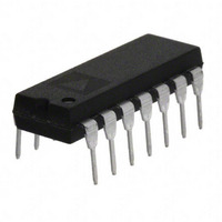
IC CONVERTER V-F/F-V 14DIP
Manufacturer
Analog Devices Inc
Type
Volt to Freq & Freq to Voltr
Datasheet
1.AD650KNZ.pdf
(20 pages)
Specifications of AD650KNZ
Frequency - Max
1MHz
Full Scale
±150ppm/°C
Linearity
±0.1%
Mounting Type
Through Hole
Package / Case
14-DIP (0.300", 7.62mm)
Frequency
1MHz
Full Scale Range
1MHz
Linearity %
0.1%
Supply Voltage Range
± 9V To ± 18V
Digital Ic Case Style
DIP
No. Of Pins
14
Peak Reflow Compatible (260 C)
Yes
Converter Function
VFC/FVC
Full Scale Frequency
1000
Power Supply Requirement
Dual
Single Supply Voltage (typ)
Not RequiredV
Single Supply Voltage (max)
Not RequiredV
Single Supply Voltage (min)
Not RequiredV
Dual Supply Voltage (min)
±9V
Dual Supply Voltage (max)
±18V
Operating Temperature (min)
0C
Operating Temperature (max)
70C
Operating Temperature Classification
Commercial
Package Type
PDIP
Converter Type
Frequency/Voltage + Voltage/Frequency
Rohs Compliant
Yes
Calibration Error Fs Typ
5%
Lead Free Status / RoHS Status
Lead free / RoHS Compliant
Lead Free Status / RoHS Status
Lead free / RoHS Compliant, Lead free / RoHS Compliant
Available stocks
Company
Part Number
Manufacturer
Quantity
Price
Company:

Part Number:
AD650KNZ
Manufacturer:
Analog Devices Inc
Quantity:
135
Company:
Part Number:
AD650KNZ
Manufacturer:
AD
Quantity:
3 012


AD650
PIN CONFIGURATIONS AND FUNCTION DESCRIPTIONS
Table 2. Pin Function Descriptions
D-14, N-14
1
2
3
4
5
6
7
8
9
10
11
12
13, 14
BIBOLAR OFFSET
Pin No.
CAPACITOR
ONE SHOT
Figure 2. D-14, N-14 Pin Configurations
CURRENT
P-20A
2
3
4
6
8
9
1, 5, 7, 10, 11, 15, 17
12
13
14
16
18
19, 20
V
OUT
–V
+IN
–IN
NC
S
1
2
3
4
5
6
7
NC = NO CONNECT
(Not to Scale)
TOP VIEW
AD650
Mnemonic
V
+IN
–IN
BIPOLAR OFFSET
CURRENT
–V
ONE-SHOT
CAPACITOR
NC
F
COMPARATOR INPUT
DIGITAL GND
ANALOG GND
+V
OFFSET NULL
14
13
12
11
10
OUTPUT
OUT
9
8
S
S
OFFSET NULL
OFFSET NULL
+V
ANALOG GND
DIGITAL GND
COMPARATOR
INPUT
F
OUTPUT
S
Rev. D | Page 6 of 20
Description
Output of Operational Amplifier. The operational amplifier, along with C
is used in the integrate stage of the V to F conversion.
Positive Analog Input.
Negative Analog Input.
On-Chip Current Source. This can be used in conjunction with an external
resistor to remove the operational amplifier’s offset.
Negative Power Supply Input.
The Capacitor, C
for the one shot.
No Connect.
Frequency Output from AD650.
Input to Comparator. When the input voltage reaches −0.6 V, the one shot is
triggered.
Digital Ground.
Analog Ground.
Positive Power Supply Input.
Offset Null Pins. Using an external potentiometer, the offset of the
operational amplifier can be removed.
OS
NC = NO CONNECT
BIPOLAR OFFSET
, is Connected to This Pin. C
CURRENT
–V
–IN
NC
NC
Figure 3. P-20A Pin Configuration
S
4
5
6
7
8
3
9
(Not to scale)
PIN 1
INDENTFIER
TOP VIEW
AD650
10
2
11
1
OS
20
12
determines the time period
19
13
18
17
16
15
14
+V
NC
ANALOG GND
NC
DIGITAL GND
S
INT
,
Related parts for AD650KNZ
Image
Part Number
Description
Manufacturer
Datasheet
Request
R

Part Number:
Description:
±1.7g Dual-Axis IMEMS Accelerometer Evaluation Board
Manufacturer:
Analog Devices Inc
Datasheet:

Part Number:
Description:
Inertial Sensor Evaluation System
Manufacturer:
Analog Devices Inc
Datasheet:
Part Number:
Description:
Manufacturer:
Analog Devices Inc
Datasheet:
Part Number:
Description:
Manufacturer:
Analog Devices Inc
Datasheet:
Part Number:
Description:
Manufacturer:
Analog Devices Inc
Datasheet:
Part Number:
Description:
Manufacturer:
Analog Devices Inc
Datasheet:
Part Number:
Description:
Manufacturer:
Analog Devices Inc
Datasheet:
Part Number:
Description:
Manufacturer:
Analog Devices Inc
Datasheet:
Part Number:
Description:
Manufacturer:
Analog Devices Inc
Datasheet:
Part Number:
Description:
Manufacturer:
Analog Devices Inc
Datasheet:
Part Number:
Description:
Manufacturer:
Analog Devices Inc
Datasheet:
Part Number:
Description:
Manufacturer:
Analog Devices Inc
Datasheet:
Part Number:
Description:
Manufacturer:
Analog Devices Inc
Datasheet: