AD650KNZ Analog Devices Inc, AD650KNZ Datasheet - Page 2
AD650KNZ
Manufacturer Part Number
AD650KNZ
Description
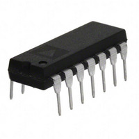
IC CONVERTER V-F/F-V 14DIP
Manufacturer
Analog Devices Inc
Type
Volt to Freq & Freq to Voltr
Datasheet
1.AD650KNZ.pdf
(20 pages)
Specifications of AD650KNZ
Frequency - Max
1MHz
Full Scale
±150ppm/°C
Linearity
±0.1%
Mounting Type
Through Hole
Package / Case
14-DIP (0.300", 7.62mm)
Frequency
1MHz
Full Scale Range
1MHz
Linearity %
0.1%
Supply Voltage Range
± 9V To ± 18V
Digital Ic Case Style
DIP
No. Of Pins
14
Peak Reflow Compatible (260 C)
Yes
Converter Function
VFC/FVC
Full Scale Frequency
1000
Power Supply Requirement
Dual
Single Supply Voltage (typ)
Not RequiredV
Single Supply Voltage (max)
Not RequiredV
Single Supply Voltage (min)
Not RequiredV
Dual Supply Voltage (min)
±9V
Dual Supply Voltage (max)
±18V
Operating Temperature (min)
0C
Operating Temperature (max)
70C
Operating Temperature Classification
Commercial
Package Type
PDIP
Converter Type
Frequency/Voltage + Voltage/Frequency
Rohs Compliant
Yes
Calibration Error Fs Typ
5%
Lead Free Status / RoHS Status
Lead free / RoHS Compliant
Lead Free Status / RoHS Status
Lead free / RoHS Compliant, Lead free / RoHS Compliant
Available stocks
Company
Part Number
Manufacturer
Quantity
Price
Company:

Part Number:
AD650KNZ
Manufacturer:
Analog Devices Inc
Quantity:
135
Company:
Part Number:
AD650KNZ
Manufacturer:
AD
Quantity:
3 012


AD650
TABLE OF CONTENTS
Features .............................................................................................. 1
Functional Block Diagram .............................................................. 1
Product Description......................................................................... 1
Product Highlights ........................................................................... 1
Revision History ............................................................................... 2
Specifications..................................................................................... 3
Absolute Maximum Ratings............................................................ 5
Pin Configurations and Function Descriptions ........................... 6
Circuit Operation ............................................................................. 7
REVISION HISTORY
3/06—Rev. C to Rev. D
Updated Format..................................................................Universal
Changes to Product Highlights....................................................... 1
Changes to Table 1............................................................................ 3
Added Pin Function Descriptions Table ...................................... 6
Updated Outline Dimensions ....................................................... 18
Changes to Ordering Guide .......................................................... 19
ESD Caution.................................................................................. 5
Unipolar Configuration............................................................... 7
Component Selection................................................................... 8
Bipolar V/F .................................................................................. 10
Unipolar V/F, Negative Input Voltage ..................................... 10
Rev. D | Page 2 of 20
Applications..................................................................................... 16
Outline Dimensions ....................................................................... 19
F/V Conversion .......................................................................... 10
High Frequency Operation ....................................................... 10
Decoupling and Grounding...................................................... 12
Temperature Coefficients.......................................................... 12
Nonlinearity Specification ........................................................ 13
PSRR............................................................................................. 14
Other Circuit Considerations ................................................... 14
Differential Voltage-to-Frequency Conversion...................... 16
Autozero Circuit......................................................................... 16
Phase-Locked Loop F/V Conversion ...................................... 17
Ordering Guide .......................................................................... 20
Related parts for AD650KNZ
Image
Part Number
Description
Manufacturer
Datasheet
Request
R

Part Number:
Description:
±1.7g Dual-Axis IMEMS Accelerometer Evaluation Board
Manufacturer:
Analog Devices Inc
Datasheet:

Part Number:
Description:
Inertial Sensor Evaluation System
Manufacturer:
Analog Devices Inc
Datasheet:
Part Number:
Description:
Manufacturer:
Analog Devices Inc
Datasheet:
Part Number:
Description:
Manufacturer:
Analog Devices Inc
Datasheet:
Part Number:
Description:
Manufacturer:
Analog Devices Inc
Datasheet:
Part Number:
Description:
Manufacturer:
Analog Devices Inc
Datasheet:
Part Number:
Description:
Manufacturer:
Analog Devices Inc
Datasheet:
Part Number:
Description:
Manufacturer:
Analog Devices Inc
Datasheet:
Part Number:
Description:
Manufacturer:
Analog Devices Inc
Datasheet:
Part Number:
Description:
Manufacturer:
Analog Devices Inc
Datasheet:
Part Number:
Description:
Manufacturer:
Analog Devices Inc
Datasheet:
Part Number:
Description:
Manufacturer:
Analog Devices Inc
Datasheet:
Part Number:
Description:
Manufacturer:
Analog Devices Inc
Datasheet: