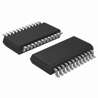
ADT7476AARQZ-REEL ON Semiconductor, ADT7476AARQZ-REEL Datasheet - Page 11

ADT7476AARQZ-REEL
Manufacturer Part Number
ADT7476AARQZ-REEL
Description
IC REMOTE THERMAL CTRLR 24-QSOP
Manufacturer
ON Semiconductor
Series
dBCool®r
Datasheet
1.ADT7476AARQZ.pdf
(67 pages)
Specifications of ADT7476AARQZ-REEL
Function
Fan Control, Temp Monitor
Topology
ADC, Comparator, Fan Speed Counter, Multiplexer, Register Bank
Sensor Type
External & Internal
Sensing Temperature
-40°C ~ 125°C, External Sensor
Output Type
SMBus™
Output Alarm
No
Output Fan
Yes
Voltage - Supply
3 V ~ 3.6 V
Operating Temperature
-40°C ~ 125°C
Mounting Type
Surface Mount
Package / Case
24-QSOP
Lead Free Status / RoHS Status
Lead free / RoHS Compliant
serial bus in one operation. However, it is not possible to mix
read and write in one operation because the type of operation
is determined at the beginning and cannot subsequently be
changed without starting a new operation. In the
ADT7476A, write operations contain either one or two
bytes, and read operations contain one byte.
data from it, the address pointer register must be set so the
correct data register is addressed. Then, data can be written
into that register or read from it. The first byte of a write
operation always contains an address stored in the address
pointer register. If data is to be written to the device, then the
write operation contains a second data byte that is written to
the register selected by the address pointer register.
address is sent over the bus, and then R/W is set to 0. This
is followed by two data bytes. The first data byte is the
address of the internal data register to be written to, which
is stored in the address pointer register. The second data byte
is the data to be written to the internal data register.
When reading data from a register, there are two
possibilities:
Figure 18. Writing a Register Address to the Address Pointer Register, then Writing Data to the Selected Register
Any number of bytes of data can be transferred over the
To write data to one of the device data registers or read
This write operation is illustrated in Figure 18. The device
clock pulse to assert a stop condition. In read
mode, the master device overrides the
acknowledge bit by pulling the data line high
during the low period before the ninth clock pulse.
This is known as no acknowledge. The master then
takes the data line low during the low period
before the 10
the 10
SDA
SCL
START BY
MASTER
th
SDA
SCL
clock pulse to assert a stop condition.
START BY
MASTER
th
1
0
clock pulse, and then high during
1
1
0
SERIAL BUS ADDRESS BYTE
Figure 19. Writing to the Address Pointer Register Only
1
0
SERIAL BUS ADDRESS BYTE
0
1
FRAME 1
1
1
FRAME 1
A1
SDA (CONTINUED)
1
SCL (CONTINUED)
http://onsemi.com
A1
A0
R/W
A0
ADT7476A
ACK. BY
11
R/W
9
ADT7476A
without first writing to the address pointer register, if the
address pointer register is already at the correct value.
However, it is not possible to write data to a register without
writing to the address pointer register, because the first data
byte of a write is always written to the address pointer
register.
protocols, the ADT7476A also supports the read byte
protocol. See Intel’s System Management Bus Specifications
Revision 2 for more information.
succession, the master can send a repeat start condition
instead of a stop condition to begin a new operation.
ACK. BY
It is possible to read a data byte from a data register
In addition to supporting the send byte and receive byte
If several read or write operations must be performed in
D7
D7
9
1
1
1. If the ADT7476A’s address pointer register value
2. If the address pointer register is already known to
is unknown, or not the desired value, then it must
first be set to the correct value before data can be
read from the desired data register. This is done by
performing a write to the ADT7476A as before,
but only the data byte containing the register
address is sent, because no data is written to the
register (see Figure 19).
A read operation is then performed consisting of
the serial bus address; R/W bit set to 1, followed
by the data byte read from the data register (see
Figure 20.)
be at the desired address, data can be read from the
corresponding data register without first writing to
the address pointer register (see Figure 20).
D7
D6
D6
1
ADDRESS POINTER REGISTER BYTE
D6
D5
D5
ADDRESS POINTER REGISTER BYTE
D5
D4
D4
DATA BYTE
FRAME 2
FRAME 3
D4
D3
D3
FRAME 2
D3
D2
D2
D2
D1
D1
D1
D0
D0
ADT7476A
ADT7476A
ACK. BY
ACK. BY
D0
9
9
ADT7476A
ACK. BY
STOP BY
MASTER
9
STOP BY
MASTER


