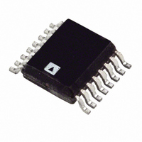
ADT7518ARQ-REEL Analog Devices Inc, ADT7518ARQ-REEL Datasheet - Page 22

ADT7518ARQ-REEL
Manufacturer Part Number
ADT7518ARQ-REEL
Description
IC SENSOR TEMP W/ADC/DAC 16QSOP
Manufacturer
Analog Devices Inc
Datasheet
1.ADT7518ARQ.pdf
(40 pages)
Specifications of ADT7518ARQ-REEL
Rohs Status
RoHS non-compliant
Function
Temp Monitoring System (Sensor)
Topology
ADC, Comparator, Multiplexer, Register Bank
Sensor Type
External & Internal
Sensing Temperature
-40°C ~ 120°C, External Sensor
Output Type
I²C™, MICROWIRE™, QSPI™, SPI™
Output Alarm
No
Output Fan
No
Voltage - Supply
2.7 V ~ 5.5 V
Operating Temperature
-40°C ~ 120°C
Mounting Type
Surface Mount
Package / Case
16-QSOP
ADT7518
AIN Interrupts
The measured results from the AIN inputs are compared with
the AIN V
equal to comparison) limits. An interrupt occurs if the AIN
inputs exceed or equal the limit registers. These voltage limits
are stored in on-chip registers. Note that the limit registers are
8 bits long while the AIN conversion result is 10 bits long. If the
voltage limits are not masked out, then any out-of-limit com-
parisons generate flags that are stored in the Interrupt Status 1
register (Address = 00h) and one or more out-of-limit results
will cause the INT/ INT output to pull either high or low
depending on the output polarity setting. It is good design
practice to mask out interrupts for channels that are of no
concern to the application. Figure 49 shows the interrupt
structure for the ADT7518. It gives a block diagram
representation of how the various measurement channels affect
the INT/ INT pin.
FUNCTIONAL DESCRIPTION—MEASUREMENT
Temperature Sensor
The ADT7518 contains an ADC with special input signal
conditioning to enable operation with external and on-chip
diode temperature sensors. When the ADT7518 is operating in
single-channel mode, the ADC continually processes the
measurement taken on one channel only. This channel is
preselected by Bits C0:C2 in the Control Configuration 2
register (Address 19h). When in round robin mode, the analog
input multiplexer sequentially selects the V
on-chip temperature sensor to measure its internal temperature,
either the external temperature sensor or AIN1 and AIN2,
AIN3, and then AIN4. These signals are digitized by the ADC
and the results are stored in the various value registers.
HIGH
(greater than comparison) and V
COMPARISONS
READ RESET
WATCHDOG
S/W RESET
LIMIT
AIN1 TO AIN4)
REGISTER 2
INTERRUPT
INTERRUPT
(TEMP AND
REGISTER
DD
STATUS
STATUS
(V
input channel, the
DD
LOW
)
(less than or
Figure 49. Interrupt Structure
CONFIGURATION
REGISTER 1
REGISTERS
INTERRUPT
Rev. A | Page 22 of 40
CONTROL
MASK
INTERNAL
TEMP
EXTERNAL
TEMP
V
DIODE
FAULT
AIN1–AIN4
The measured results from the temperature sensors are com-
pared with the internal and external T
temperature limits are stored in on-chip registers. If the temp-
erature limits are not masked, any out-of-limit comparisons
generate flags that are stored in the Interrupt Status 1 register.
One or more out-of-limit results will cause the INT/ INT output
to pull either high or low depending on the output polarity
setting.
Theoretically, the temperature measuring circuit can measure
temperatures from –128°C to +127°C with a resolution of
0.25°C. However, temperatures outside T
guaranteed operating temperature range of the device. Temp-
erature measurement from –128°C to +127°C is possible using
an external sensor.
Temperature measurement is initiated by three methods. The
first method is applicable when the part is in single-channel
measurement mode. The temperature is measured 16 times and
internally averaged to reduce noise. In single-channel mode, the
part is continuously monitoring the selected channel, i.e., as
soon as one measurement is taken another one is started on the
same channel. The total time to measure a temperature channel
with the ADC operating at slow speed is typically 11.4 ms
(712 µs × 16) for the internal temperature sensor and 24.22 ms
(1.51 ms × 16) for the external temperature sensor. The new
temperature value is stored in two 8-bit registers and is ready
for reading by the I
of disabling the averaging by setting Bit 5 in the Control
Configuration 2 register (Address 19h). The ADT7518 defaults
on power-up with averaging enabled.
DD
ENABLE BIT
INT/INT
2
C or SPI interface. The user has the option
INT/INT
(LATCHED OUTPUT)
HIGH
A
, T
are outside the
LOW
limits. These


