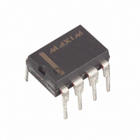
DS1624+ Maxim Integrated Products, DS1624+ Datasheet - Page 4

DS1624+
Manufacturer Part Number
DS1624+
Description
IC THERM/EEPROM DIG 256BYTE 8DIP
Manufacturer
Maxim Integrated Products
Datasheet
1.DS1624S.pdf
(17 pages)
Specifications of DS1624+
Function
Thermometer, Thermostat
Topology
EEPROM, Register Bank
Sensor Type
Internal
Sensing Temperature
-55°C ~ 125°C
Output Type
2-Wire Serial
Output Alarm
No
Output Fan
No
Voltage - Supply
2.7 V ~ 5.5 V
Operating Temperature
-55°C ~ 125°C
Mounting Type
Through Hole
Package / Case
8-DIP (0.300", 7.62mm)
Full Temp Accuracy
+/- 0.5 C
Digital Output - Bus Interface
2-Wire, SMBus
Digital Output - Number Of Bits
13 bit
Supply Voltage (max)
5.5 V
Supply Voltage (min)
2.7 V
Maximum Operating Temperature
+ 125 C
Minimum Operating Temperature
- 55 C
Supply Current
1000 uA
Lead Free Status / RoHS Status
Lead free / RoHS Compliant
Data valid: The state of the data line represents valid data when, after a START condition, the data line
is stable for the duration of the HIGH period of the clock signal. The data on the line must be changed
during the LOW period of the clock signal. There is one clock pulse per bit of data.
Each data transfer is initiated with a START condition and terminated with a STOP condition The
number of data bytes transferred between START and STOP conditions is not limited, and is determined
by the master device. The information is transferred byte–wise and each receiver acknowledges with a
ninth bit.
Within the bus specifications a regular mode (100 KHz clock rate) and a fast mode (400 KHz clock rate)
are defined. The DS1624 works in both modes.
Acknowledge: Each receiving device, when addressed, is obliged to generate an acknowledge after the
reception of each byte. The master device must generate an extra clock pulse which is associated with this
acknowledge bit.
A device that acknowledges must pull down the SDA line during the acknowledge clock pulse in such a
way that the SDA line is stable LOW during the HIGH period of the acknowledge related clock pulse. Of
course, setup and hold times must be taken into account. A master must signal an end of data to the slave
by not generating an acknowledge bit on the last byte that has been clocked out of the slave. In this case,
the slave must leave the data line HIGH to enable the master to generate the STOP condition.
DATA TRANSFER ON 2-WIRE SERIAL BUS Figure 2
Figure 2 details how data transfer is accomplished on the two–wire bus. Depending upon the state of the
R/
1. Data transfer from a master transmitter to a slave receiver. The first byte transmitted by the
2. Data transfer from a slave transmitter to a master receiver. The first byte (the slave
W
master is the slave address. Next follows a number of data bytes. The slave returns an acknowledge
bit after each received byte.
address) is transmitted by the master. The slave then returns an acknowledge bit. Next follows a
number of data bytes transmitted by the slave to the master. The master returns an acknowledge bit
after all received bytes other than the last byte. At the end of the last received byte, a ‘not
acknowledge’ is returned.
bit, two types of data transfer are possible:
4 of 17
DS1624


