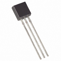
DS18B20+PAR Maxim Integrated Products, DS18B20+PAR Datasheet - Page 6

DS18B20+PAR
Manufacturer Part Number
DS18B20+PAR
Description
IC THERM MICROLAN PROG-RES TO-92
Manufacturer
Maxim Integrated Products
Specifications of DS18B20+PAR
Function
Thermometer, Thermostat
Topology
Register Bank, Scratchpad
Sensor Type
Internal
Sensing Temperature
-55°C ~ 100°C
Output Type
1-Wire®
Output Alarm
Yes
Output Fan
No
Voltage - Supply
3 V ~ 5.5 V
Operating Temperature
-55°C ~ 100°C
Mounting Type
Through Hole
Package / Case
TO-92-3 (Standard Body), TO-226
Temperature Threshold
Programmable
Full Temp Accuracy
+/- 0.5 C
Digital Output - Bus Interface
1-Wire
Digital Output - Number Of Bits
12 bit
Supply Voltage (max)
5.5 V
Supply Voltage (min)
3 V
Maximum Operating Temperature
+ 125 C
Minimum Operating Temperature
- 55 C
Supply Current
1.5 mA
Lead Free Status / RoHS Status
Lead free / RoHS Compliant
DS18B20-PAR MEMORY MAP Figure 6
CONFIGURATION REGISTER
Byte 4 of the scratchpad memory contains the configuration register, which is organized as illustrated in
Figure 7. The user can set the conversion resolution of the DS18B20-PAR using the R0 and R1 bits in
this register as shown in Table 3.
resolution). Note that there is a direct tradeoff between resolution and conversion time. Bit 7 and bits 0-4
in the configuration register are reserved for internal use by the device and cannot be overwritten.
CONFIGURATION REGISTER Figure 7
THERMOMETER RESOLUTION CONFIGURATION Table 3
CRC GENERATION
CRC bytes are provided as part of the DS18B20-PAR’s 64-bit ROM code and in the 9
scratchpad memory. The ROM code CRC is calculated from the first 56 bits of the ROM code and is
contained in the most significant byte of the ROM. The scratchpad CRC is calculated from the data
stored in the scratchpad, and therefore it changes when the data in the scratchpad changes. The CRCs
provide the bus master with a method of data validation when data is read from the DS18B20-PAR. To
verify that data has been read correctly, the bus master must re-calculate the CRC from the received data
byte 0 Temperature LSB (50h)
byte 1 Temperature MSB (05h)
byte 2 T
byte 3 T
byte 4 Configuration Register*
byte 5 Reserved (FFh)
byte 6 Reserved
byte 7 Reserved (10h)
byte 8 CRC*
SCRATCHPAD (Power-up State)
*
in EEPROM
Power-up state depends on value(s) stored
H
L
R1
0
0
1
1
Register or User Byte 2*
Register or User Byte 1*
bit 7
0
R0
0
1
0
1
bit 6
R1
The power-up default of these bits is R0 = 1 and R1 = 1 (12-bit
Resolution
bit 5
R0
10-bit
11-bit
12-bit
9-bit
bit 4
(85°C)
1
6 of 19
bit 3
Max Conversion Time
1
93.75 ms
187.5 ms
375 ms
750 ms
bit 2
1
T
T
H
L
Configuration Register
bit 1
Register or User Byte 2
Register or User Byte 1
1
(t
(t
(t
(t
CONV
CONV
CONV
CONV
EEPROM
bit 0
/8)
/4)
/2)
1
)
th
DS18B20-PAR
byte of the


