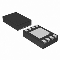
SE97TP,147 NXP Semiconductors, SE97TP,147 Datasheet - Page 43

SE97TP,147
Manufacturer Part Number
SE97TP,147
Description
IC TEMP SENSOR DIMM 8-HWSON
Manufacturer
NXP Semiconductors
Datasheet
1.SE97TK118.pdf
(55 pages)
Specifications of SE97TP,147
Function
Temp Monitoring System (Sensor)
Topology
ADC (Sigma Delta), Comparator, Register Bank
Sensor Type
Internal
Sensing Temperature
-40°C ~ 125°C
Output Type
I²C™/SMBus™
Output Alarm
Yes
Output Fan
Yes
Voltage - Supply
3 V ~ 3.6 V
Operating Temperature
-40°C ~ 125°C
Mounting Type
Surface Mount
Package / Case
8-WSON (Exposed Pad), 8-HWSON
Lead Free Status / RoHS Status
Lead free / RoHS Compliant
Other names
568-4730-2
935286725147
935286725147
NXP Semiconductors
Table 30.
V
The AC specifications fully meet or exceed SMBus 2.0 specifications, but allow the bus to interface with the I
to 400 kHz.
[1]
[2]
[3]
[4]
[5]
[6]
[7]
[8]
SE97_7
Product data sheet
Symbol
f
t
t
t
t
t
t
t
t
t
t
t
t
t
t
t
t
EEPROM power-up timing
t
t
Write cycle limits
T
SCL
HIGH
LOW
to(SMBus)
r
f
SU;DAT
h(i)(D)
HD;DAT
SU;STA
HD;STA
SU;STO
BUF
SP
VD;DAT
f(o)
POR
pu(R)
pu(W)
DD
cy(W)
= 1.7 V to 3.6 V; T
Minimum clock frequency is 0 kHz if SMBus Time-out is disabled.
Delay from SDA STOP to SDA START.
A device must internally provide a hold time of at least 200 ns for SDA signal (referenced to the V
undefined region of the falling edge of SCL.
Delay from SCL HIGH-to-LOW transition to SDA edges.
Delay from SCL LOW-to-HIGH transition to restart SDA.
Delay from SDA START to first SCL HIGH-to-LOW transition.
These parameters tested initially and after a design or process change that affects the parameter.
t
pu(R)
and t
Parameter
SCL clock frequency
HIGH period of the SCL clock 70 % to 70 %
LOW period of the SCL clock 30 % to 30 %
SMBus time-out time
rise time of both SDA and
SCL signals
fall time of both SDA and SCL
signals
data set-up time
data input hold time
data hold time
set-up time for a repeated
START condition
hold time (repeated) START
condition
set-up time for STOP
condition
bus free time between a
STOP and START condition
pulse width of spikes that
must be suppressed by the
input filter
data valid time
output fall time
power-on reset pulse time
read power-up time
write power-up time
write cycle time
SMBus AC characteristics
pu(W)
are the delays required from the time V
amb
=
[7]
−
40
°
C to +125
Conditions
LOW period to reset
SMBus
30 % of SDA to
70 % of SCL
from clock
power supply falling
°
C; unless otherwise specified. These specifications are guaranteed by design.
Rev. 07 — 29 January 2010
DDR memory module temp sensor with integrated SPD, 3.3 V
DD
is stable until the specified operation can be initiated.
[2][3]
[4]
[5]
[6]
[2]
[8]
[8]
[9]
Standard mode
4000
4700
4700
4000
4000
4700
10
Min
250
200
200
0.5
25
0
-
-
-
-
-
-
-
[1]
1000
3450
Max
100
300
35
50
10
1
1
-
-
-
-
-
-
-
-
-
-
-
IH(min)
of the SCL signal) to bridge the
1300
1300
10
Min
200
600
100
200
600
600
600
0.5
Fast mode
25
20
0
-
-
-
-
-
-
[1]
© NXP B.V. 2010. All rights reserved.
2
C-bus from DC
Max
400
300
300
900
250
35
50
10
SE97
1
1
-
-
-
-
-
-
-
-
-
-
43 of 55
Unit
kHz
ns
ns
ns
ns
ns
ns
ns
ns
ns
ns
ns
ns
ns
μs
ms
ms
ms
ms
ns


