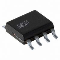
LM75AD,112 NXP Semiconductors, LM75AD,112 Datasheet - Page 11

LM75AD,112
Manufacturer Part Number
LM75AD,112
Description
IC TEMP SENSOR DIGITAL 8-SOIC
Manufacturer
NXP Semiconductors
Datasheet
1.LM75ADP118.pdf
(24 pages)
Specifications of LM75AD,112
Package / Case
8-SOIC (3.9mm Width)
Function
Temp Sensor, Watchdog
Topology
ADC (Sigma Delta), Comparator, Oscillator, Register Bank
Sensor Type
Internal
Sensing Temperature
-55°C ~ 125°C
Output Type
I²C™
Output Alarm
No
Output Fan
Yes
Voltage - Supply
2.8 V ~ 5.5 V
Operating Temperature
-55°C ~ 125°C
Mounting Type
Surface Mount
Lead Free Status / RoHS Status
Lead free / RoHS Compliant
For Use With
OM6285 - EVAL BOARD I2C-2002-1A568-4002 - DEMO BOARD I2C
Lead Free Status / Rohs Status
Lead free / RoHS Compliant
Other names
568-4226-5
935269775112
LM75AD
LM75AD
935269775112
LM75AD
LM75AD
NXP Semiconductors
LM75A_4
Product data sheet
7.10 Protocols for writing and reading the registers
When the power supply voltage is dropped below the device power-on reset level of
approximately 1.9 V (POR) and then rises up again, the device will be reset to its default
condition as listed above.
The communication between the host and the LM75A must strictly follow the rules as
defined by the I
operations are illustrated in
10. A’: master acknowledge bit, not returned by the device, but set by the master or host
11. NA: Not Acknowledge bit. During this clock period, both the device and host release
12. In a write protocol, data is sent from the host to the device and the host controls the
13. In a read protocol, data is sent to the bus by the device and the host must release the
1. Before a communication, the I
2. The host must provide SCL clock pulses necessary for the communication. Data is
3. During data transfer, except the START and STOP signals, the SDA signal must be
4. S: START signal, initiated by the host to start a communication, the SDA goes from
5. RS: RE-START signal, same as the START signal, to start a read command that
6. P: STOP signal, generated by the host to stop a communication, the SDA goes from
7. W: write bit, when the write/read bit = LOW in a write command.
8. R: read bit, when the write/read bit = HIGH in a read command.
9. A: device acknowledge bit, returned by the LM75A. It is LOW if the device works
and SDA lines must both be released by all devices on the bus, and they become
HIGH by the bus pull-up resistors.
transferred in a sequence of 9 SCL clock pulses for every 8-bit data byte followed by
1-bit status of the acknowledgement.
stable while the SCL signal is HIGH. It means that the SDA signal can be changed
only during the LOW duration of the SCL line.
HIGH to LOW while the SCL is HIGH.
follows a write command.
LOW to HIGH while the SCL is HIGH. The bus becomes free thereafter.
properly and HIGH if not. The host must release the SDA line during this period in
order to give the device the control on the SDA line.
in reading 2-byte data. During this clock period, the host must set the SDA line to
LOW in order to notify the device that the first byte has been read for the device to
provide the second byte onto the bus.
the SDA line at the end of a data transfer, the host is then enabled to generate the
STOP signal.
SDA line, except during the clock period when the device sends the device
acknowledgement signal to the bus.
SDA line during the time that the device is providing data onto the bus and controlling
the SDA line, except during the clock period when the master sends the master
acknowledgement signal to the bus.
2
C-bus management. The protocols for LM75A register read/write
Rev. 04 — 10 July 2007
Figure 5
2
C-bus must be free or not busy. It means that the SCL
Digital temperature sensor and thermal watchdog
to
Figure 10
together with the following definitions:
© NXP B.V. 2007. All rights reserved.
LM75A
11 of 24


