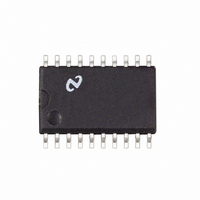
LM2635MX National Semiconductor, LM2635MX Datasheet - Page 8

LM2635MX
Manufacturer Part Number
LM2635MX
Description
IC REG SYNCH BUCK 5-BIT 20-SOIC
Manufacturer
National Semiconductor
Datasheet
1.LM2635MNOPB.pdf
(13 pages)
Specifications of LM2635MX
Applications
Power Supplies
Current - Supply
2.5mA
Voltage - Supply
4.5 V ~ 5.5 V
Operating Temperature
0°C ~ 125°C
Mounting Type
Surface Mount
Package / Case
20-SOIC (7.5mm Width)
Lead Free Status / RoHS Status
Lead free / RoHS Compliant
Other names
*LM2635MX
LM2635MXTR
LM2635MXTR
Available stocks
Company
Part Number
Manufacturer
Quantity
Price
Company:
Part Number:
LM2635MX
Manufacturer:
FUJITSU
Quantity:
2
Part Number:
LM2635MX
Manufacturer:
NS/国半
Quantity:
20 000
Company:
Part Number:
LM2635MX/NOPB
Manufacturer:
NXP
Quantity:
3 050
www.national.com
Applications Information
output voltage level is fed to the error amplifier. The output of
the
internally generated PWM ramp signal and the result of the
comparison is a series of pulses with certain duty ratios.
These pulses are used to control the turn-on and turn-off of
the MOSFET gate drivers. In this way, the error in the output
voltage gets “compensated” or cancelled by the change in
the duty ratio of the FET switches. During a large load
transient, depending on the compensation design, the
change in duty ratio can be as fast as less than one switch-
ing cycle. Refer to Design Considerations section for more
details.
Besides the usual voltage mode feedback control loop, the
LM2635 also has a pair of fast comparators (the MIN and
MAX comparators) to help maintain the output voltage dur-
ing a large and fast load transient. The trip points of the
comparators are set to
When the load transient is so large that the output voltage
goes outside the
will bypass the primary voltage control loop and immediately
set the duty ratio to either maximum value or to zero. This
provides the fastest possible way to react to such a large
load transient in a classical buck converter.
Power Good Signal
The power good signal is used to indicate that the output
voltage is within specified range. In the LM2635, the range is
set to a
start, the power good signal is always low. At the end of the
soft start session,the output voltage is checked and the
PWRGD pin will be asserted if the voltage is within specified
range.
Over Voltage Protection
When the output voltage exceeds 115% of the DAC output
voltage after the end of soft start, the LM2635 will enter over
voltage protection mode in which it shuts itself down. The
upper gate driver is held low while the lower gate driver is
held high. PWRGD will be low. For LM2635 to recover from
OVP mode, either OUTEN or V
Another more subtle way to recover is to float all the VID pins
and reapply the correct code.
Current Limit
Current limit is realized by sensing the V
high side MOSFET when it is on. Since the r
MOSFET is a known value, current through the MOSFET
can be known by monitoring V
the three parameters is:
To implement the current limit function, an external resistor
R
the drain of the high side MOSFET and the IMAX pin. A
constant current of around 180 µA is forced into the IMAX pin
and causes a fixed voltage drop across the R
This voltage drop is then compared with the V
side MOSFET and if the latter is higher, over current is
reached. So the appropriate value of R
determined current limit level I
following equation:
IMAX
error
is need. The resistor should be connected between
±
10% window of the DAC output voltage. During soft
amplifier
±
5% window, the MIN or MAX comparator
is
±
5% of the DAC output voltage.
then
DS
LIM
CC
. The relationship between
voltage has to be toggled.
can be calculated by the
compared
DS
IMAX
(Continued)
voltage of the
DS
IMAX
DS_ON
for a pre-
of the high
with
resistor.
of a
an
8
For example, if we know that the r
20 mΩ, and the current limit we want to set is 20A, then we
should choose the value of R
To provide the greatest protection over the high side MOS-
FET, cycle by cycle protection is implemented. The sampling
of the V
turned on. Whenever an over current condition is detected,
the high side switch is immediately turned off and the low
side switch turned on, until the next switching cycle comes.
The delay of 300 ns is to circumvent switching noise when
the MOSFET is first turned on.
DESIGN CONSIDERATIONS
Control Loop Compensation
A switching regulator should be properly compensated to
achieve a stable condition. For a synchronous buck regula-
tor that needs to meet stringent load transient requirement
such as a Pentium II MPU core voltage supply, a simple
2-pole-1-zero compensation network should suffice, such as
the one shown in Figure 4 (C
because the ESR zero of the typical output capacitors is low
enough to make the control-to-output transfer function a
single-pole-roll-off.
As an example, let us figure out the values of the compen-
sation network components in Figure 4. Assume the follow-
ing parameters: R = 20Ω, R
C = 7.5 mF, V
= 300 kH. These parameters are based on the typical appli-
cation in Figure 1. Notice R
resistance and the on resistance of the MOSFETs.
FIGURE 4. Buck Converter from a Control Point of
DS
starts as early as about 300 ns after the switch is
IN
= 5V, V
m
View
L
L
= 2V and switching frequency
= 20 mΩ, R
IMAX
is the sum of the inductor DC
1
, C
DS_ON
to be 2.2 kΩ.
2
, R
C
1
of the MOSFET is
= 9 mΩ, L = 2 µH,
and R
2
). This is
10011909


