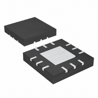
MAX8890ETCDDD+ Maxim Integrated Products, MAX8890ETCDDD+ Datasheet - Page 6

MAX8890ETCDDD+
Manufacturer Part Number
MAX8890ETCDDD+
Description
IC POWER MANAGE CELL 12-TQFN
Manufacturer
Maxim Integrated Products
Datasheet
1.MAX8890ETCAAAT.pdf
(12 pages)
Specifications of MAX8890ETCDDD+
Applications
Handheld/Mobile Devices
Current - Supply
180µA
Voltage - Supply
2.5 V ~ 5.5 V
Operating Temperature
-40°C ~ 85°C
Mounting Type
Surface Mount
Package / Case
12-TQFN Exposed Pad
Product
Charge Management
Battery Type
Li-Ion, Li-Polymer
Operating Supply Voltage
2.5 V to 5.5 V
Supply Current
180 uA
Maximum Operating Temperature
+ 85 C
Minimum Operating Temperature
- 40 C
Charge Safety Timers
No
Mounting Style
SMD/SMT
Temperature Monitoring
No
Uvlo Start Threshold
2.25 V
Uvlo Stop Threshold
2.25 V
Lead Free Status / RoHS Status
Lead free / RoHS Compliant
Integrated Cellular RF-Section
Power-Management IC
(Circuit of Figure 1, MAX8890ETCGGG, V
6
_______________________________________________________________________________________
PIN
EP
10
11
12
1
2
3
4
5
6
7
8
9
NAME
OUT2
OUT3
OUT1
GND
GND
GND
A. V
B. V
C. V
D. I
V
EN1
EN2
EN3
IN1
IN2
IN3
BP
IN
IN
= 3.3V, EN2 = EN3 = GND, C
EN1
OUT1
BP
, 200mA/div
= 1.25V, 1V/div
= 0 to 3.3V, 5V/div
= 2.8V, R
ENABLE WAVEFORM
Regulator 1 Input. Supply voltage can range from 2.5V to 5.5V. Bypass with a capacitor to GND (see
Capacitor Selection and Regulator Stability section).
Regulator 2 Input. Supply voltage can range from 2.5V to V
Capacitor Selection and Regulator Stability section).
Regulator 2 Output. Sources up to 100mA. Bypass with a 2.2µF ceramic capacitor to GND.
Active-High Enable Input for Regulator 1. A logic low shuts down the first linear regulator. In shutdown,
OUT1 is pulled low through an internal 5k resistor. Connect to IN1 for normal operation.
Active-High Enable Input for Regulator 2. A logic low shuts down the second linear regulator. In
shutdown, OUT2 is pulled low through an internal 5k resistor. Connect to IN2 for normal operation.
Active-High Enable Input for Regulator 3. A logic low shuts down the third linear regulator. In
shutdown, OUT3 is pulled low through an internal 5k resistor. Connect to IN3 for normal operation.
1.25V Voltage Reference Bypass Pin. Connect a 0.01µF ceramic bypass capacitor from BP to GND to
minimize the output noise. Make no other connection to this pin.
Ground. Connect both ground pins together externally, as close to the IC as possible.
Regulator 3 Input. Supply voltage can range from 2.5V to V
Capacitor Selection and Regulator Stability section).
Regulator 3 Output. Sources up to 100mA. Bypass with a 2.2µF ceramic capacitor to GND.
Ground. Connect both ground pins together externally, as close to the IC as possible.
Regulator 1 Output. Sources up to 100mA. Bypass with a 2.2µF ceramic capacitor to GND.
Gr ound . T H E EXPO SED PA D A N D A L L F O U R C O R N ER T A B S O N T H E Q F N PA C K A G E A R E
IN T ER N A L L Y C O N N EC T ED TO G R O U N D . The exp osed p ad functi ons as a heatsi nk. S ol d er to a l ar g e
p ad or to the ci r cui t b oar d g r ound p l ane to m axi m i ze p ow er d i ssi p ati on. D o not use as d evi ce g r ound .
(1ST OUTPUT)
OUT1
20 s/div
= 28 (100mA), 2V/div
BP
= 0.01 F
IN
= 3.3V, EN_ = IN_, T
MAX8890 toc16
Typical Operating Characteristics (continued)
C
B
D
A
A
= +25°C, unless otherwise noted.)
FUNCTION
A. V
B. V
C. V
D. I
V
IN
IN
EN2
OUT2
= 3.3V, EN1 = IN, EN3 = GND, C
BP
, 200mA/div
= 1.25V, 1V/div
= 0 to 3.3V, 5V/div
IN1
IN1
= 2.8V, R
ENABLE WAVEFORM
. Bypass with a capacitor to GND (see
. Bypass with a capacitor to GND (see
(2ND OUTPUT)
OUT2
20 s/div
= 28 (100mA), 2V/div
BP
Pin Description
= 0.01 F
MAX8890 toc17
C
B
D
A


